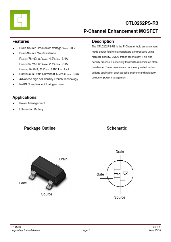
CTL0262PS-R3 Overview
The CTL0262PS-R3 is the P-Channel logic enhancement mode power field effect transistors are produced using high cell density, DMOS trench technology. This high density process is especially tailored to minimize on-state resistance. These devices are particularly suited for low voltage application such as cellular phone and notebook puter power management.
CTL0262PS-R3 Key Features
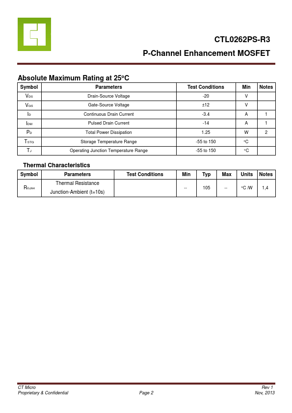
- Drain-Source Breakdown Voltage VDSS -20 V
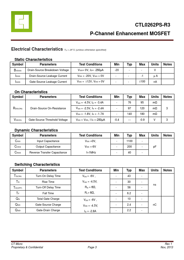
- Drain-Source On-Resistance
- Continuous Drain Current at TC=25℃ID = -3.4A
- Advanced high cell density Trench Technology
- RoHS pliance & Halogen Free