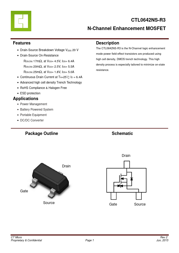
Datasheet4U Logo Datasheet4U.com

CTL0642NS-R3 - N-Channel MOSFET

General Description

The CTL0642NS-R3 is the N-Channel logic enhancement mode power field effect transistors are produced using high cell density, DMOS trench technology.

This high density process is especially tailored to minimize on-state resistance.

Key Features

  • Drain-Source Breakdown Voltage VDSS 20 V.
  • Drain-Source On-Resistance RDS(ON) 17mΩ, at VGS= 4.5V, IDS= 6.4A RDS(ON) 20mΩ, at VGS= 2.5V, IDS= 5.5A RDS(ON) 25mΩ, at VGS= 1.8V, IDS= 5.0A ℃.
  • Continuous Drain Current at TA=25 ID = 6.4A.
  • Advanced high cell density Trench Technology.
  • RoHS Compliance & Halogen Free.
  • ESD protection.

📥 Download Datasheet

Datasheet Details

Part number CTL0642NS-R3
Manufacturer CT Micro
File Size 1.96 MB
Description N-Channel MOSFET
Datasheet download datasheet CTL0642NS-R3 Datasheet

Full PDF Text Transcription (Reference)

The following content is an automatically extracted verbatim text from the original manufacturer datasheet and is provided for reference purposes only.

View original datasheet text
CTL0642NS-R3 N-Channel Enhancement MOSFET Features • Drain-Source Breakdown Voltage VDSS 20 V • Drain-Source On-Resistance RDS(ON) 17mΩ, at VGS= 4.5V, IDS= 6.4A RDS(ON) 20mΩ, at VGS= 2.5V, IDS= 5.5A RDS(ON) 25mΩ, at VGS= 1.8V, IDS= 5.0A ℃• Continuous Drain Current at TA=25 ID = 6.4A • Advanced high cell density Trench Technology • RoHS Compliance & Halogen Free • ESD protection Applications • Power Management • Battery Powered System • Portable Equipment • DC/DC Converter Package Outline Description The CTL0642NS-R3 is the N-Channel logic enhancement mode power field effect transistors are produced using high cell density, DMOS trench technology. This high density process is especially tailored to minimize on-state resistance.