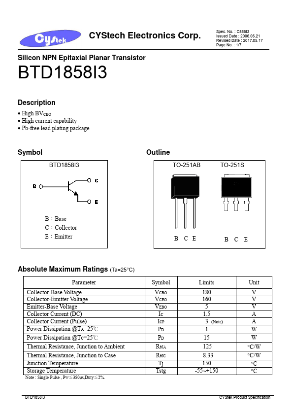
High BVCEO
High current capability
Pb-free lead plating package
Symbol
BTD1858I3
Outline
TO-251AB
TO-251S
B:Base C:Collector E:Emitter
B CE
BCE
Absolute Maximum Ratings (Ta=25°C)
Parameter Collector-Base Voltage Collector-Emitter Voltage Emitter-Base Voltage Colle
Full PDF Text Transcription for BTD1858I3 (Reference)
Note: Below is a high-fidelity text extraction (approx. 800 characters) for
BTD1858I3. For precise diagrams, and layout, please refer to the original PDF.
d Date : 2006.06.21 Revised Date : 2017.05.17 Page No. : 1/7 Description • High BVCEO • High current capability • Pb-free lead plating package Symbol BTD1858I3 Outline TO-251AB TO-251S B:Base C:Collector E:Emitter B CE BCE Absolute Maximum Ratings (Ta=25°C) Parameter Collector-Base Voltage Collector-Emitter Voltage Emitter-Base Voltage Collector Current (DC) Collector Current (Pulse) Power Dissipation @TA=25℃ Power Dissipation @TC=25℃ Thermal Resistance, Junction to Ambient Thermal Resistance, Junction to Case Junction Temperature Storage Temperature Note : Single Pulse , Pw≦380μs,Duty≦2%. BTD1858I3 Symbol VCBO VCEO VEBO I