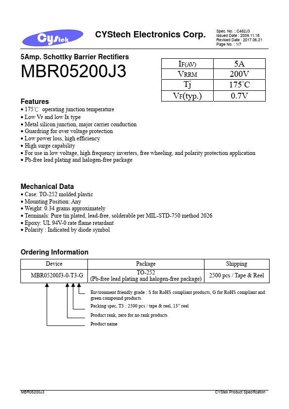
Equivalent Circuit
MBR05200J3
CYStech Electronics Corp.
Spec. No. : C462J3
Issued Date : 2009.11.18
Revised Date : 2017.06.21
Page No. : 2/7
Outline
TO-252(DPAK)
AKA
Maximum Ratings and Electrical Characteristics
(Rating at 25°C ambient temperature unless otherwise specified. Single phase, half wave, 60Hz,
resistive or inductive load. For capacitive load, derate current by 20%.)
Parameter
Maximum Recurrent peak reverse voltage
Maximum RMS voltage
Maximum DC blocking voltage
Maximum instantaneous IF=5A, TC=25℃
forward voltage at
(Note 1)
IF=5A, TC=125℃
Maximum Average forward rectified current
@ TC=133℃
Peak repetitive forward current (square wave,
20kHz, TC=133℃)
Non-repetitive peak forward surge current @
8.3ms single half sine wave superimposed on
rated load (JEDEC method)
Peak repetitive reverse surge current (Note 1 ), TJ<175℃
Maximum instantaneous VR=200 V, TC=25℃
reverse current at
VR=200 V, TC=125℃
Voltage rate of change, (rated VR)
Typical junction capacitance @ f=1MHz and applied
5V reverse voltage
ESD susceptibility (Note 2)
Storage temperature range
Operating junction temperature range
Notes : 1. 2.0μs pulse width, f=1.0kHz
2. Human body model, 1.5kΩ in series with 100pF
Symbol
VRRM
VRMS
VDC
VF
IF(AV)
IFRM
IFSM
IRRM
IR
dV/dt
CJ
Tstg
TJ
Value
200
140
200
0.90
0.74
5
10
110
2
5
5
10,000
65 (typ.)
8000
Units
V
V
V
V
A
A
A
A
μA
mA
V/μs
pF
V
℃
℃
MBR05200J3
CYStek Product Specification