MTB20N04J3
Features
RDSON(TYP)
VGS=10V, ID=10A VGS=4.5V, ID=8A
- Low Gate Charge
- Simple Drive Requirement
- Pb-free lead plating package
40V 23A 16.3A 17.5mΩ 20.8mΩ
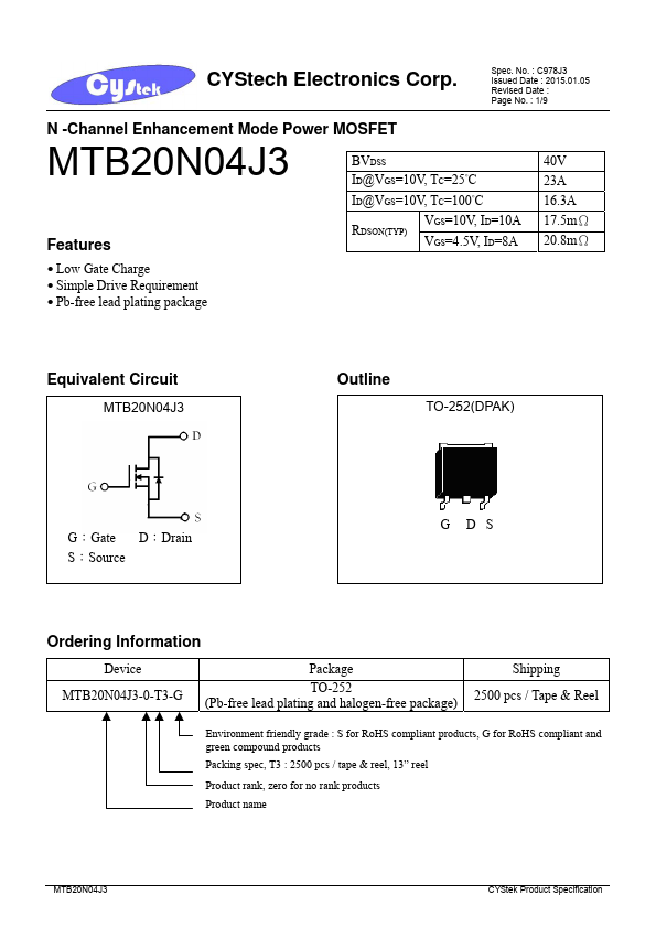
Equivalent Circuit
Outline
TO-252(DPAK)
G:Gate D:Drain S:Source
G DS
Ordering Information
Device MTB20N04J3-0-T3-G
Package
TO-252 (Pb-free lead plating and halogen-free package)
Shipping 2500 pcs / Tape & Reel
Environment friendly grade : S for Ro HS pliant products, G for Ro HS pliant and green pound products Packing spec, T3 : 2500 pcs / tape & reel, 13” reel
Product rank, zero for no rank products
Product name
CYStek Product Specification
CYStech Electronics Corp.
Absolute Maximum Ratings (TC=25°C, unless otherwise noted)
Parameter
Drain-Source Voltage Gate-Source Voltage
Continuous Drain Current @ TC=25°C, VGS=10V Continuous Drain Current @ TC=100°C, VGS=10V Pulsed Drain Current
- 1 Avalanche Current Avalanche Energy @ L=1m H, ID=18A, RG=25Ω Total Power Dissipation @TC=25℃ Total Power...