Datasheet4U.com
🌙
MTD5D0C03J4 Datasheet | CYStech
Part:
MTD5D0C03J4
Description:
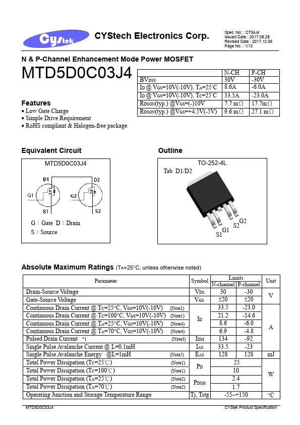
N- & P-Channel Logic Level Enhancement Mode Power MOSFET
Category:
MOSFET
Manufacturer:
CYStech
Size:
540.40 KB
MTD5D0C03J4 Datasheet (PDF) Download
CYStech
MTD5D0C03J4
Key Features
Low Gate Charge RDSON(typ.) @VGS=+4.5V(-5V)
Simple Drive Requirement
RoHS compliant & Halogen-free package
×
Close