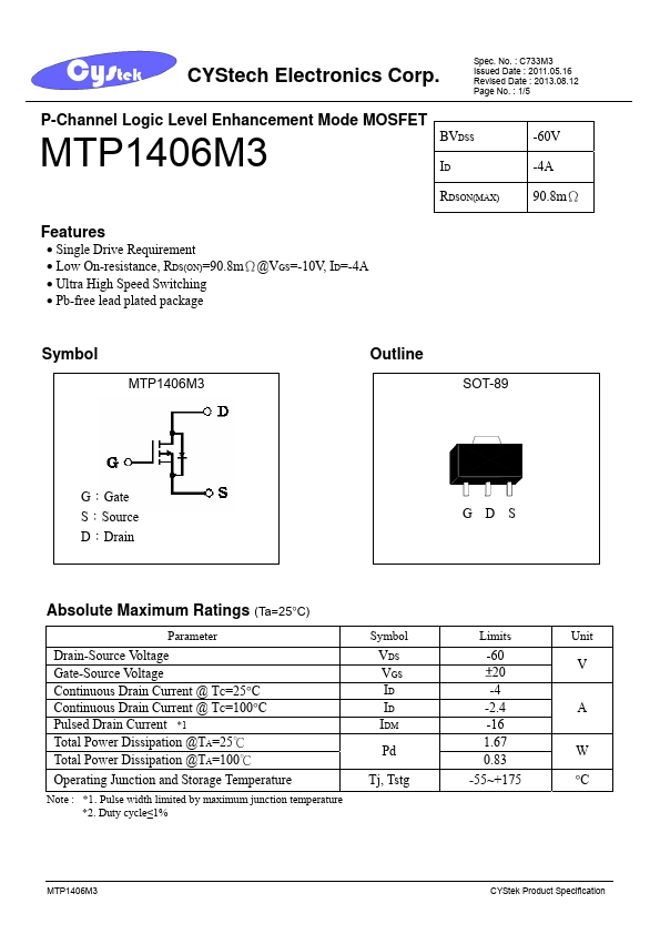
Datasheet4U Logo Datasheet4U.com

MTP1406M3 - P-Channel Logic Level Enhancement Mode MOSFET

Key Features

  • Single Drive Requirement.
  • Low On-resistance, RDS(ON)=90.8mΩ@VGS=-10V, ID=-4A.
  • Ultra High Speed Switching.
  • Pb-free lead plated package BVDSS ID RDSON(MAX) -60V -4A 90.8mΩ Symbol MTP1406M3 Outline SOT-89 G:Gate S:Source D:Drain G D D S Absolute Maximum Ratings (Ta=25°C) Parameter Symbol Limits Unit Drain-Source Voltage Gate-Source Voltage Continuous Drain Current @ TC=25°C Continuous Drain Current @ TC=100°C Pulsed Drain Current.
  • 1 Total Power Dissi.

📥 Download Datasheet

Datasheet Details

Part number MTP1406M3
Manufacturer CYStech Electronics
File Size 278.20 KB
Description P-Channel Logic Level Enhancement Mode MOSFET
Datasheet download datasheet MTP1406M3 Datasheet

Full PDF Text Transcription for MTP1406M3 (Reference)

Note: Below is a high-fidelity text extraction (approx. 800 characters) for MTP1406M3. For precise diagrams, and layout, please refer to the original PDF.

CYStech Electronics Corp. P-Channel Logic Level Enhancement Mode MOSFET Spec. No. : C733M3 Issued Date : 2011.05.16 Revised Date : 2013.08.12 Page No. : 1/5 MTP1406M3 Fea...

View more extracted text
te : 2011.05.16 Revised Date : 2013.08.12 Page No. : 1/5 MTP1406M3 Features • Single Drive Requirement • Low On-resistance, RDS(ON)=90.8mΩ@VGS=-10V, ID=-4A • Ultra High Speed Switching • Pb-free lead plated package BVDSS ID RDSON(MAX) -60V -4A 90.8mΩ Symbol MTP1406M3 Outline SOT-89 G:Gate S:Source D:Drain G D D S Absolute Maximum Ratings (Ta=25°C) Parameter Symbol Limits Unit Drain-Source Voltage Gate-Source Voltage Continuous Drain Current @ TC=25°C Continuous Drain Current @ TC=100°C Pulsed Drain Current *1 Total Power Dissipation @TA=25℃ Total Power Dissipation @TA=100℃ Operating Junction and Storage Temperature Note :