MTP2010J3
Features
- Low Gate Charge
- Simple Drive Requirement
- Pb-free lead plating and halogen-free package
BVDSS ID RDSON(MAX)
-100V -20A 95mΩ @ VGS=-10V, ID=-10A 105mΩ@ VGS=-4.5V, ID=-10A
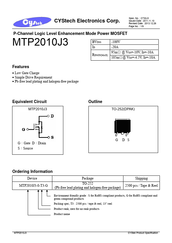
Equivalent Circuit
Outline
TO-252(DPAK)
G:Gate D:Drain S:Source
Ordering Information
Device MTP2010J3-0-T3-G Package TO-252 (Pb-free lead plating and halogen-free package) Shipping 2500 pcs / Tape & Reel
Environment friendly grade : S for Ro HS pliant products, G for Ro HS pliant and green pound products Packing spec, T3 : 2500 pcs / tape & reel, 13” reel Product rank, zero for no rank products Product name
CYStek Product Specification http://..
CYStech Electronics Corp.
Absolute Maximum Ratings (TC=25°C, unless otherwise noted)
Parameter Symbol
Spec. No. : C732J3 Issued Date : 2011.11.10 Revised Date : 2013.12.26 Page No. : 2/9
Limits
Unit
Drain-Source Voltage Gate-Source Voltage Continuous Drain Current @ TC=25°C Continuous Drain Current @ TC=100°C Pulsed Drain...