MTP2301V3 Description
CYStech Electronics Corp. -20V P-CHANNEL Enhancement Mode MOSFET Spec. 2012.07.18 Revised Date.
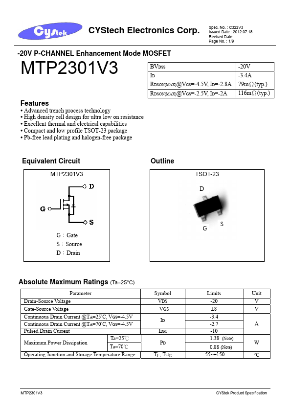
MTP2301V3 Key Features
- Advanced trench process technology
- High density cell design for ultra low on resistance
- Excellent thermal and electrical capabilities
- pact and low profile TSOT-23 package
- Pb-free lead plating and halogen-free package
- 20V -3.4A 79mΩ(typ.) 116mΩ(typ.)