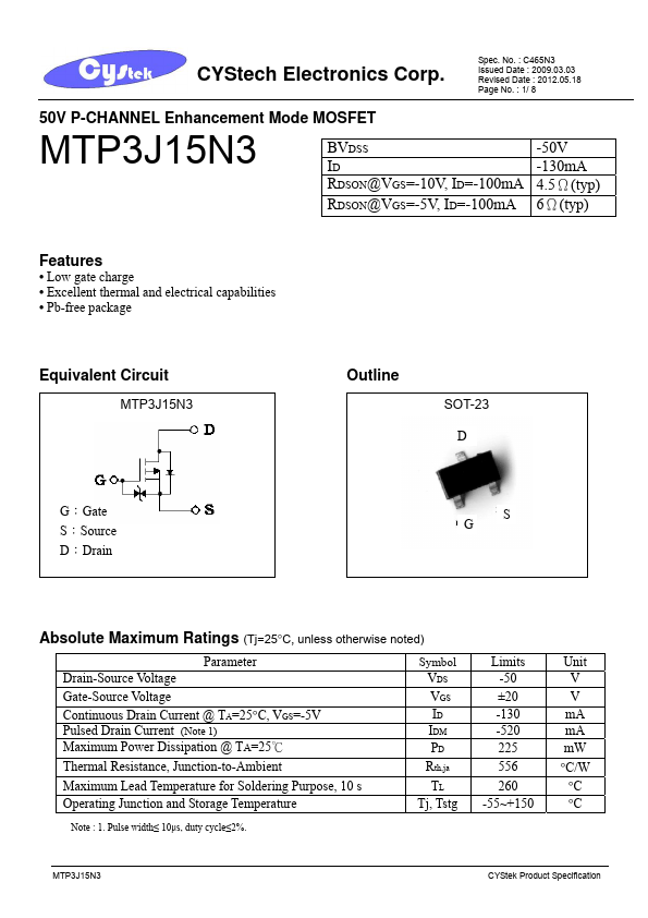
MTP3J15N3 Description
CYStech Electronics Corp. 50V P-CHANNEL Enhancement Mode MOSFET Spec. 2009.03.03 Revised Date.
MTP3J15N3 Key Features
- Low gate charge
- Excellent thermal and electrical capabilities
- Pb-free package
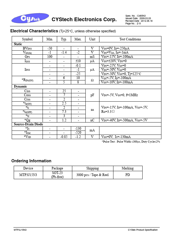
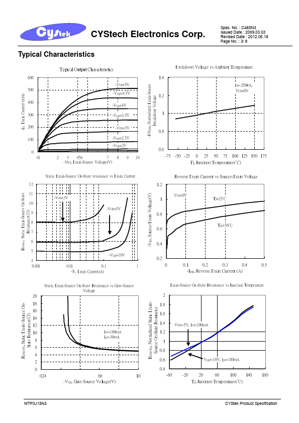
- 50V -130mA 4.5Ω(typ) 6Ω(typ)
MTP3J15N3 is 50V P-CHANNEL Enhancement Mode MOSFET manufactured by CYStech Electronics.
CYStech Electronics Corp. 50V P-CHANNEL Enhancement Mode MOSFET Spec. 2009.03.03 Revised Date.