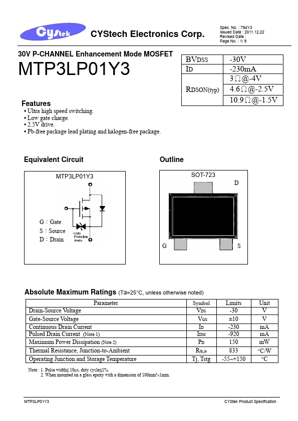
Datasheet4U Logo Datasheet4U.com

MTP3LP01Y3 - 30V P-CHANNEL Enhancement Mode MOSFET

Key Features

  • Ultra high speed switching.
  • Low gate charge.
  • 2.5V drive.
  • Pb-free package lead plating and halogen-free package. BVDSS ID RDSON(typ) -30V -230mA 3Ω@-4V 4.6Ω@-2.5V 10.9Ω@-1.5V Equivalent Circuit MTP3LP01Y3 Outline SOT-723 D G:Gate S:Source D:Drain G S Absolute Maximum Ratings (Ta=25°C, unless otherwise noted) Parameter Drain-Source Voltage Gate-Source Voltage Continuous Drain Current Pulsed Drain Current (Note 1) Maximum Power Dissipation (Note 2) Th.

📥 Download Datasheet

Datasheet Details

Part number MTP3LP01Y3
Manufacturer CYStech Electronics
File Size 377.71 KB
Description 30V P-CHANNEL Enhancement Mode MOSFET
Datasheet download datasheet MTP3LP01Y3 Datasheet

Full PDF Text Transcription for MTP3LP01Y3 (Reference)

Note: Below is a high-fidelity text extraction (approx. 800 characters) for MTP3LP01Y3. For precise diagrams, and layout, please refer to the original PDF.

CYStech Electronics Corp. 30V P-CHANNEL Enhancement Mode MOSFET Spec. No. : 794Y3 Issued Date : 2011.12.22 Revised Date : Page No. : 1/ 8 MTP3LP01Y3 Features • Ultra high...

View more extracted text
.12.22 Revised Date : Page No. : 1/ 8 MTP3LP01Y3 Features • Ultra high speed switching. • Low gate charge. • 2.5V drive. • Pb-free package lead plating and halogen-free package. BVDSS ID RDSON(typ) -30V -230mA 3Ω@-4V 4.6Ω@-2.5V 10.9Ω@-1.5V Equivalent Circuit MTP3LP01Y3 Outline SOT-723 D G:Gate S:Source D:Drain G S Absolute Maximum Ratings (Ta=25°C, unless otherwise noted) Parameter Drain-Source Voltage Gate-Source Voltage Continuous Drain Current Pulsed Drain Current (Note 1) Maximum Power Dissipation (Note 2) Thermal Resistance, Junction-to-Ambient Operating Junction and Storage Temperature Note : 1. Pulse width≤ 10μs, du