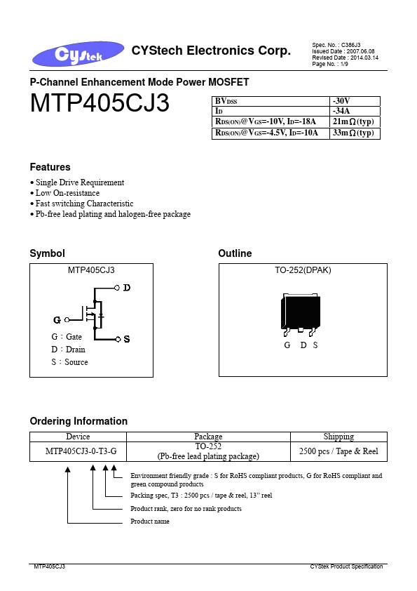
MTP405CJ3 - P-Channel Enhancement Mode Power MOSFET
CYStech Electronics
Key Features
Single Drive Requirement.
Low On-resistance.
Fast switching Characteristic.
Pb-free lead plating and halogen-free package
BVDSS ID RDS(ON)@VGS=-10V, ID=-18A RDS(ON)@VGS=-4.5V, ID=-10A
-30V -34A 21mΩ(typ) 33mΩ(typ)
Symbol
MTP405CJ3
Outline
TO-252(DPAK)
G:Gate D:Drain S:Source
G
D S
Ordering Information
Device MTP405CJ3-0-T3-G Package TO-252 (Pb-free lead plating package) Shipping 2500 pcs / Tape & Reel
Environment friendly grade : S for RoHS compliant.
Full PDF Text Transcription for MTP405CJ3 (Reference)
Note: Below is a high-fidelity text extraction (approx. 800 characters) for
MTP405CJ3. For precise diagrams, and layout, please refer to the original PDF.
CYStech Electronics Corp. P-Channel Enhancement Mode Power MOSFET Spec. No. : C386J3 Issued Date : 2007.06.08 Revised Date : 2014.03.14 Page No. : 1/9 MTP405CJ3 Features ...
View more extracted text
007.06.08 Revised Date : 2014.03.14 Page No. : 1/9 MTP405CJ3 Features • Single Drive Requirement • Low On-resistance • Fast switching Characteristic • Pb-free lead plating and halogen-free package BVDSS ID RDS(ON)@VGS=-10V, ID=-18A RDS(ON)@VGS=-4.
 MTP405CJ3 Datasheet