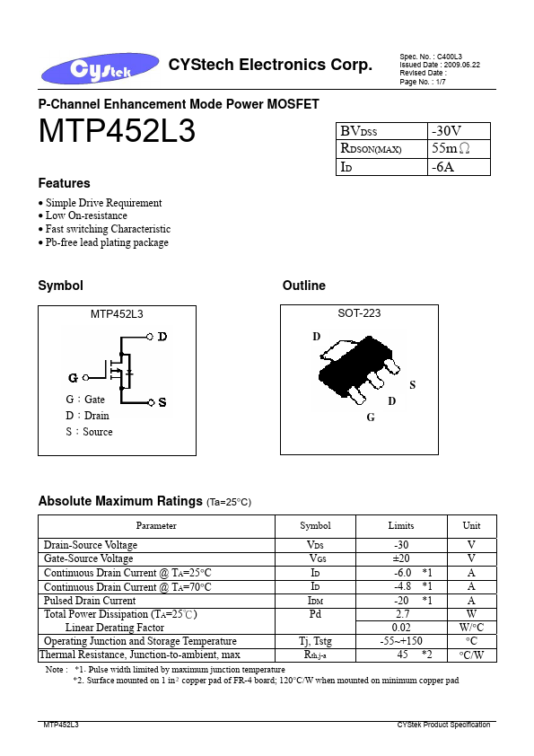
MTP452L3 Description
CYStech Electronics Corp. P-Channel Enhancement Mode Power MOSFET Spec. 2009.06.22 Revised Date.
MTP452L3 Key Features
- Simple Drive Requirement
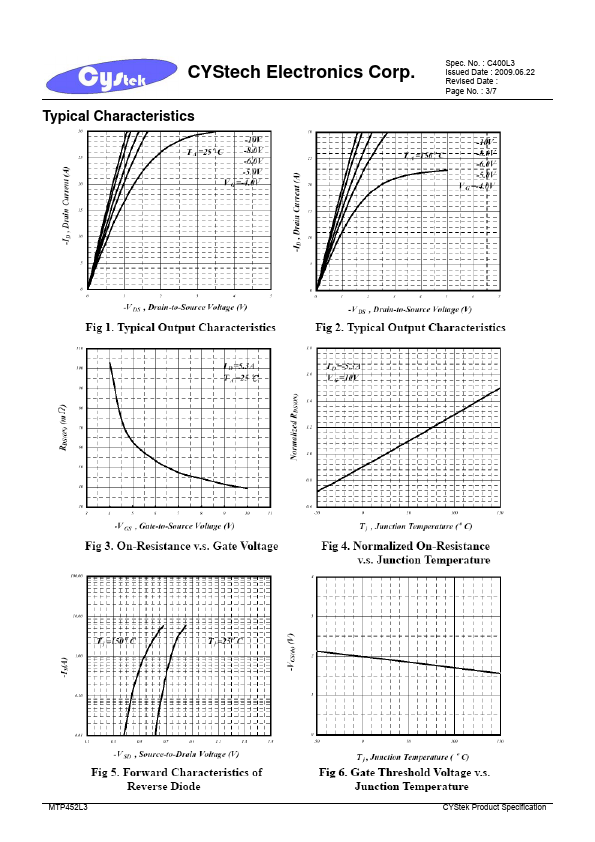
- Low On-resistance
- Fast switching Characteristic
- Pb-free lead plating package
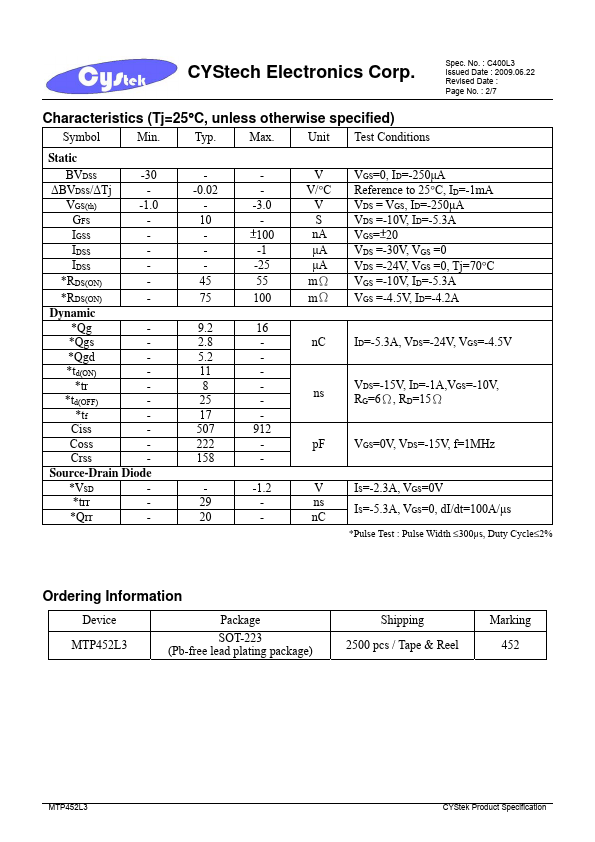
- 30V 55mΩ -6A