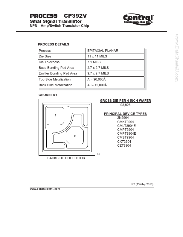
CP392V Description
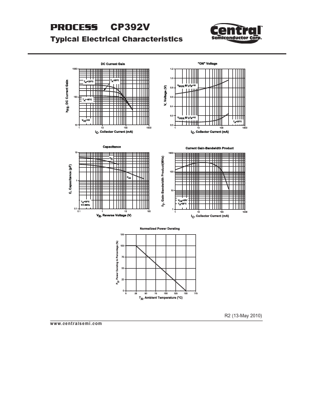
PROCESS Smal Signal Transistor CP392V NPN - Amp/Switch Transistor Chip .. c o m PROCESS CP392V Typical R2 (13-May 2010) w w.
CP392V Key Features
- s e m i . c o m PROCESS CP392V Typical
CP392V is NPN Transistor manufactured by Central Semiconductor.
| Manufacturer | Part Number | Description |
|---|---|---|
| CP39236H | PELTIER MODULE |
PROCESS Smal Signal Transistor CP392V NPN - Amp/Switch Transistor Chip .. c o m PROCESS CP392V Typical R2 (13-May 2010) w w.