CP555 Description
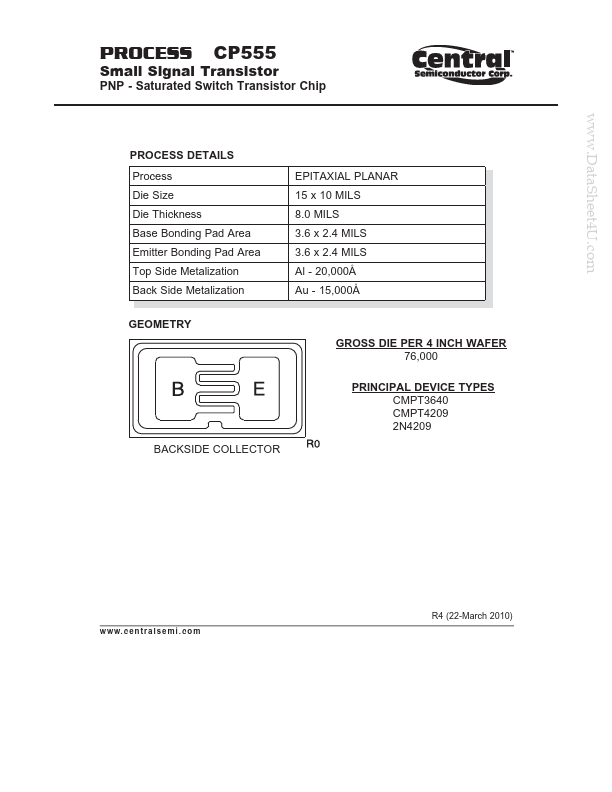
PROCESS Small Signal Transistor PNP - Saturated Switch Transistor Chip CP555 .. c o m PROCESS CP555 Typical R4 (22-March 2010) w w.
CP555 Key Features
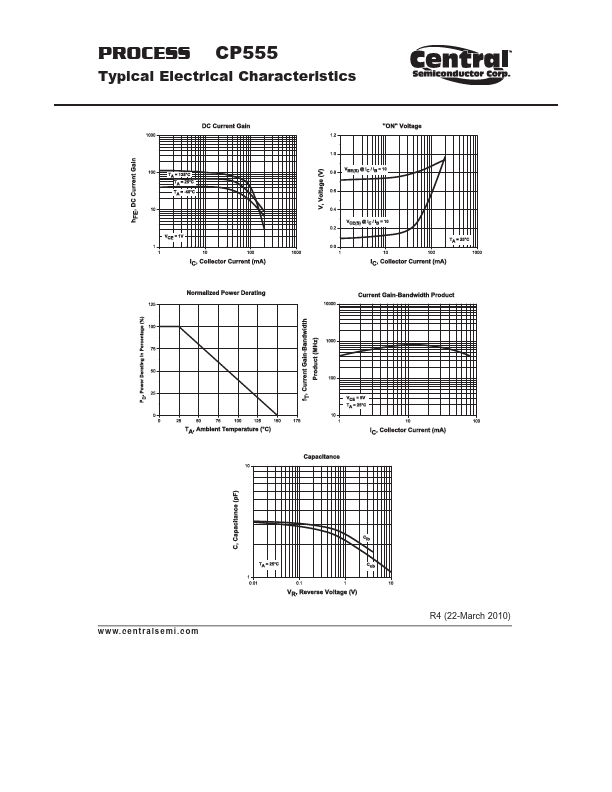
- s e m i . c o m PROCESS CP555 Typical
CP555 is PNP Transistor manufactured by Central Semiconductor.
| Part Number | Description |
|---|---|
| CP54 | Power Transistor PNP |
| CP576 | PNP Amp / Switch Transistor Chip |
| CP588 | PNP Transistor |
| CP591 | Small Signal Transistor PNP - Amp/Switch Transistor Chip |
| CP591V | PNP Transistor |
PROCESS Small Signal Transistor PNP - Saturated Switch Transistor Chip CP555 .. c o m PROCESS CP555 Typical R4 (22-March 2010) w w.