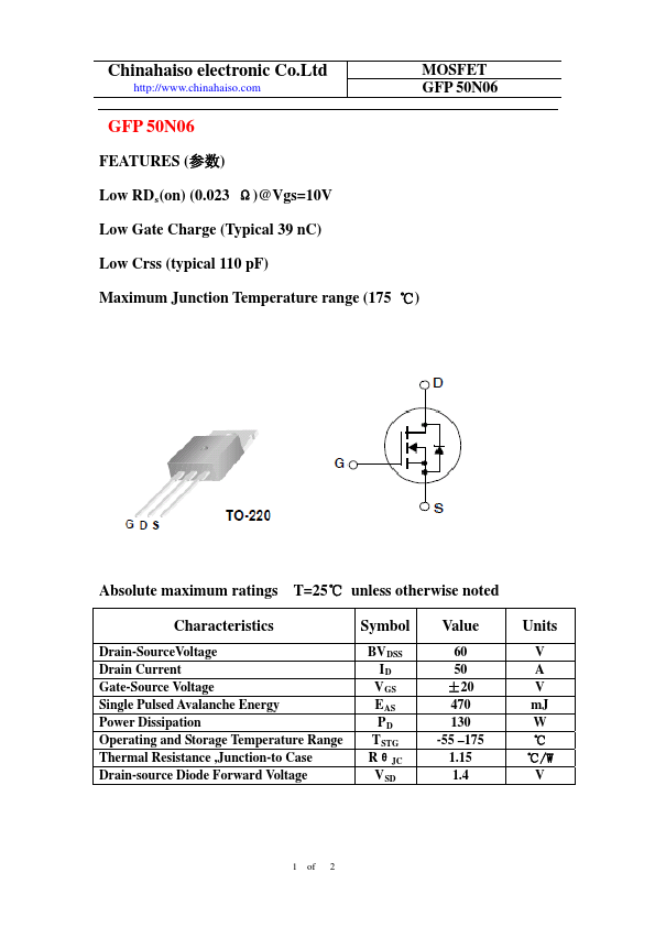
() Low RD s (on) (0.023 Ω)@Vgs=10V Low Gate Charge (Typical 39 nC) Low Crss (typical 110 pF) Maximum Junction Temperature range (175 ℃)
Absolute maximum ratings Characteristics
T=25℃ unless otherwise noted Symbol
BV DSS ID V GS E AS PD T STG Rθ JC V SD
Value
60 50 ±20 470 130 -55.
175 1.15 1.4
Units
V A V mJ W ℃ ℃/W V
Drain-SourceVoltage Drain Current Gate-Source Voltage Single Pulsed Avalanche Energy Power Dissipation Operating and Storage Temperature Range Thermal Resistance ,Junc.
Full PDF Text Transcription for GFP50N06 (Reference)
Note: Below is a high-fidelity text extraction (approx. 800 characters) for
GFP50N06. For precise diagrams, and layout, please refer to the original PDF.
s (on) (0.023 Ω)@Vgs=10V Low Gate Charge (Typical 39 nC) Low Crss (typical 110 pF) Maximum Junction Temperature range (175 ℃) Absolute maximum ratings Characteristics T=25℃ unless otherwise noted Symbol BV DSS ID V GS E AS PD T STG Rθ JC V SD Value 60 50 ±20 470 130 -55 –175 1.15 1.4 Units V A V mJ W ℃ ℃/W V Drain-SourceVoltage Drain Current Gate-Source Voltage Single Pulsed Avalanche Energy Power Dissipation Operating and Storage Temperature Range Thermal Resistance ,Junction-to Case Drain-source Diode Forward Voltage 1 of 2 http://www.Datasheet4U.com Chinahaiso electronic Co.Ltd http://www.chinahaiso.com MOSFET GFP 50N0