CH7308B-TF-TR
Features
- -
- -
- -
- -
- -
- -
- -
General Description
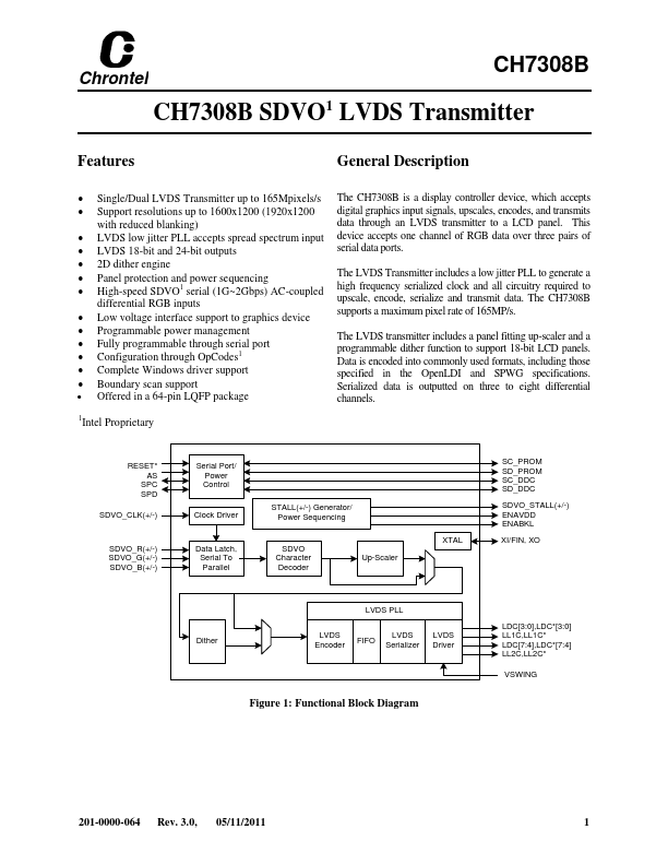
The CH7308B is a display controller device, which accepts digital graphics input signals, upscales, encodes, and transmits data through an LVDS transmitter to a LCD panel. This device accepts one channel of RGB data over three pairs of serial data ports. The LVDS Transmitter includes a low jitter PLL to generate a high frequency serialized clock and all circuitry required to upscale, encode, serialize and transmit data. The CH7308B supports a maximum pixel rate of 165MP/s. The LVDS transmitter includes a panel fitting up-scaler and a programmable dither function to support 18-bit LCD panels. Data is encoded into monly used formats, including those specified in the Open LDI and SPWG specifications. Serialized data is outputted on three to eight differential channels.
Single/Dual LVDS Transmitter up to 165Mpixels/s Support resolutions up to 1600x1200 (1920x1200 with reduced blanking) LVDS low jitter PLL accepts spread spectrum...