CMB100N03 Description
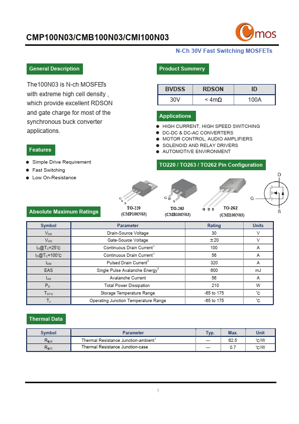
The100N03 is N-ch MOSFETs with extreme high cell density , which provide excellent RDSON and gate charge for most of the synchronous buck converter applications.
CMB100N03 is N-Ch 30V Fast Switching MOSFETs manufactured by Cmos.
| Part Number | Description |
|---|---|
| CMB100N04 | N-Ch 40V Fast Switching MOSFETs |
| CMB1404 | N-Channel Enhancement Mode Field Effect Transistor |
| CMB1405 | N-Channel Enhancement Mode Field Effect Transistor |
| CMB150N03 | N-Channel MOSFET |
| CMB3205A | N-Channel Enhancement Mode Field Effect Transistor |
The100N03 is N-ch MOSFETs with extreme high cell density , which provide excellent RDSON and gate charge for most of the synchronous buck converter applications.