CY23EP05 Overview
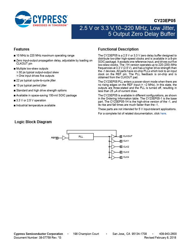
The CY23EP05 is a 2.5 V or 3.3 V zero delay buffer designed to distribute low-jitter high-speed clocks and is available in a 8-pin SOIC package. It accepts one reference input, and drives out five low-skew clocks. The -1H version operates up to 220 (200) MHz frequencies at 3.3 V (2.5 V), and has a higher drive strength than the -1 devices.
CY23EP05 Key Features
- 10 MHz to 220 MHz maximum operating range
- Zero input-output propagation delay, adjustable by loading on
- Multiple low-skew outputs
- 30 ps typical output-output skew
- One input drives five outputs
- 22 ps typical cycle-to-cycle jitter
- 13 ps typical period jitter
- Standard and high drive strength options
- Available in space-saving 150-mil SOIC package
- 3.3 V or 2.5 V operation