Full PDF Text Transcription for CY7C277 (Reference)
Note: Below is a high-fidelity text extraction (approx. 800 characters) for
CY7C277. For precise diagrams, and layout, please refer to the original PDF.
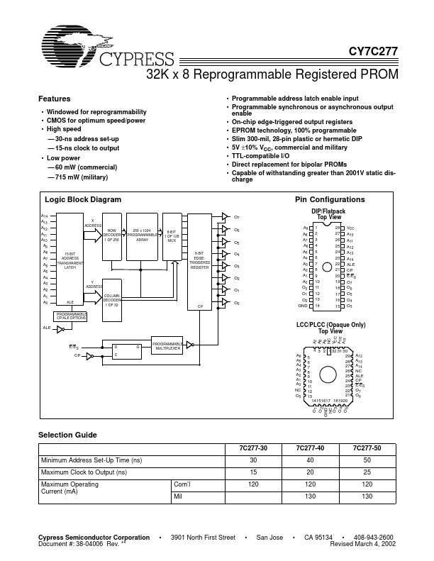
77 CY7C277 32K x 8 Reprogrammable Registered PROM Features • Windowed for reprogrammability • CMOS for optimum speed/power • High speed — 30-ns address set-up — 15-ns clo...
View more extracted text
or optimum speed/power • High speed — 30-ns address set-up — 15-ns clock to output • Low power — 60 mW (commercial) — 715 mW (military) • Programmable address latch enable input • Programmable synchronous or asynchronous output enable • On-chip edge-triggered output registers • EPROM technology, 100% programmable • Slim 300-mil, 28-pin plastic or hermetic DIP • 5V ±10% VCC, commercial and military • TTL-compatible I/O • Direct replacement for bipolar PROMs • Capable of withstanding greater than 2001V static discharge Logic Block Diagram A14 A13 X A12 A11 ADDRESS ROW DECODER 256 x 1024 PROGRAMMABLE 8-BIT 1 OF 128 A10 1 OF 2