C9827H
C9827H is High Performance Pentium 4 Clock Synthesizer manufactured by Cypress.
..
Approved Product
High Performance Pentium® 4 Clock Synthesizer
Product Features
- -
- Supports Pentium 4 Type CPUs 3.3 Volt Power Supply 10 Copies of PCI Clocks
®
- -
- -
- -
3 Differential CPU Clocks SMBus Support with Read-back Capabilities Spread Spectrum EMI Reduction Dial-a-Frequency™ Features
Dial-a-dB™ Features
56 Pin SSOP and TSSOP Package
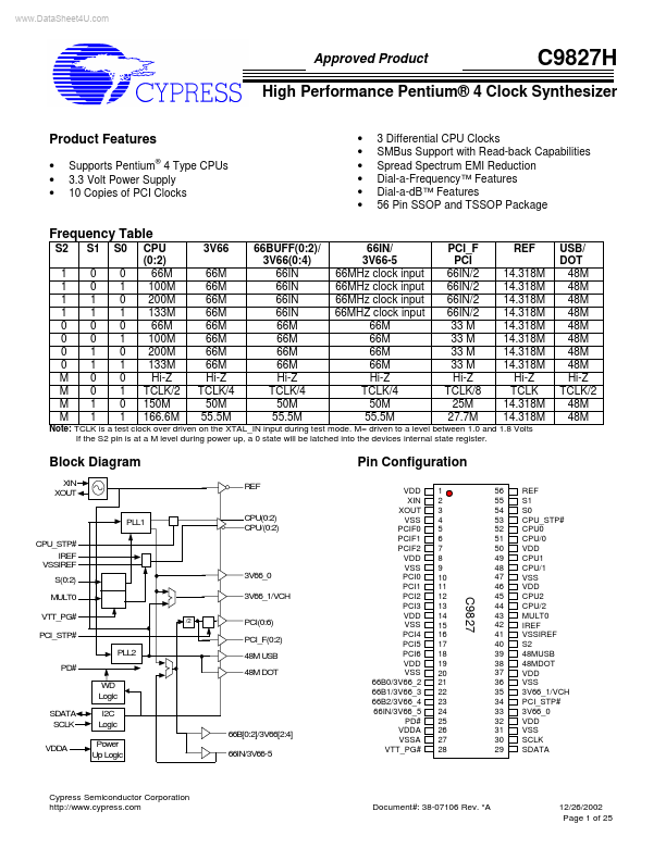
Frequency Table
S2 1 1 1 1 0 0 0 0 M M M M S1 0 0 1 1 0 0 1 1 0 0 1 1 S0 0 1 0 1 0 1 0 1 0 1 0 1 CPU (0:2) 66M 100M 200M 133M 66M 100M 200M 133M Hi-Z TCLK/2 150M 166.6M 3V66 66M 66M 66M 66M 66M 66M 66M 66M Hi-Z TCLK/4 50M 55.5M 66BUFF(0:2)/ 3V66(0:4) 66IN 66IN 66IN 66IN 66M 66M 66M 66M Hi-Z TCLK/4 50M 55.5M 66IN/...