C9870G
C9870G is Clock Synthesizer manufactured by Cypress.
Features
- -
- Supports Pentium 4 Type CPUs 3.3 Volt Power Supply 10 Copies of PCI Clocks
®
- -
- -
- -
3 Differential CPU Clocks SMBus Support with Read-back Capabilities Spread Spectrum EMI Reduction Dial-a-Frequency™ Features
Dial-a-d B™ Features
56 Pin SSOP and TSSOP Package
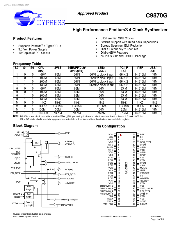
Frequency Table
S2 1 1 1 1 0 0 0 0 M M M M S1 0 0 1 1 0 0 1 1 0 0 1 1 S0 0 1 0 1 0 1 0 1 0 1 0 1 CPU (0:2) 66M 100M 200M 133M 66M 100M 200M 133M Hi-Z TCLK/2 150M 166.6M 3V66 66M 66M 66M 66M 66M 66M 66M 66M Hi-Z TCLK/4 50M 55.5M 66BUFF(0:2)/ 3V66(0:4) 66IN 66IN 66IN 66IN 66M 66M 66M 66M Hi-Z TCLK/4 50M 55.5M 66IN/ 3V66-5 66MHz clock input 66MHz clock input 66MHz clock input 66MHZ clock input 66M 66M 66M 66M Hi-Z TCLK/4 50M 55.5M PCI_F PCI 66IN/2 66IN/2 66IN/2 66IN/2 33 M 33 M 33 M 33 M Hi-Z TCLK/8 25M 27.7M REF 14.318M 14.318M 14.318M 14.318M 14.318M 14.318M 14.318M 14.318M Hi-Z TCLK 14.318M 14.318M USB/ DOT 48M 48M 48M 48M 48M 48M 48M 48M Hi-Z TCLK/2 48M 48M
Note: TCLK is a test clock over driven on the XTAL_IN input during test mode. M= driven to a level between 1.0 and 1.8 Volts If the S2 pin is at a M level during power up, a 0 state will be latched into the devices internal state register.
Block Diagram
XIN XOUT PLL1 CPU_STP# IREF VSSIREF S(0:2) MULT0 VTT_PG# PCI_STP# PLL2 PD# WD Logic SDATA SCLK VDDA I2C Logic 66B[0:2]/3V66[2:4] Power Up Logic 66IN/3V66-5
/2
Pin Configuration
VDD XIN XOUT VSS PCIF0 PCIF1 PCIF2 VDD VSS PCI0 PCI1 PCI2 PCI3 VDD VSS PCI4 PCI5 PCI6 VDD VSS 66B0/3V66_2 66B1/3V66_3 66B2/3V66_4 66IN/3V66_5 PD# VDDA VSSA VTT_PG# 1 2 3 4 5 6 7 8 9 10 11 12 13 14 15 16 17 18 19 20 21 22 23 24 25 26 27 28 56 55 54 53 52 51 50 49 48 47 46 45 44 43 42 41 40 39 38 37 36 35 34 33 32 31 30 29 REF S1 S0 CPU_STP# CPU0 CPU/0 VDD CPU1 CPU/1 VSS VDD CPU2 CPU/2 MULT0 IREF VSSIREF S2 48MUSB 48MDOT VDD VSS 3V66_1/VCH PCI_STP# 3V66_0 VDD VSS SCLK SDATA
CPU(0:2) CPU/(0:2)
3V66_0 3V66_1/VCH PCI(0:6) PCI_F(0:2) 48M USB 48M DOT
Cypress Semiconductor Corporation http://.cypress....