CB664
Overview
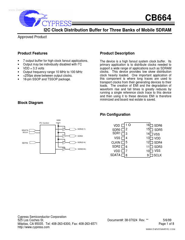
This pin is connected to the input reference clock. This clock be in the range of 10.0 to 100.0 MHz Low Skew output clock. 2 Serial data of I C-wire control interface.
- 7 output buffer for high clock fanout applications. 2 Output may be individually disabled with I C VDD = 3.3 volts Output frequency range 10 MHz to 100 MHz <250ps skew between output clocks. 16-pin SSOP and TSSOP package. Product Description The device is a high fanout system clock buffer. Its primary application is to distribute clocks needed to support a wide range of applications such as SDRAM clocks. This device provides low skew distribution clock heavily loaded. One important application of this component is where long traces are used to transport clocks from their generating devices to their loads. The creation of EMI and the degradation of waveform rise and fall times is greatly reduces by running a single reference clock trace to this device and then using it to these devices EMI is therefore minimized and board real estate is saved.