CY22701
Key Features
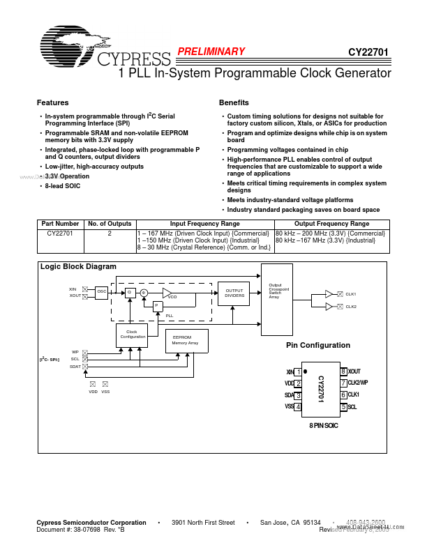
- In-system programmable through I2C Serial Programming Interface (SPI)
- Programmable SRAM and non-volatile EEPROM memory bits with 3.3V supply
- Integrated, phase-locked loop with programmable P and Q counters, output dividers
- Low-jitter, high-accuracy outputs
- 3.3V Operation
- 8-lead SOIC Benefits
- Custom timing solutions for designs not suitable for factory custom silicon, Xtals, or ASICs for production
- Program and optimize designs while chip is on system board
- Programming voltages contained in chip
- High-performance PLL enables control of output frequencies that are customizable to support a wide range of applications