CY2305C
Key Features
- 10 MHz to 100-133 MHz operating range
- Zero input and output propagation delay
- Multiple low skew outputs
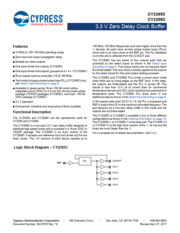
- One input drives five outputs (CY2305C)
- One input drives nine outputs, grouped as 4 + 4 + 1 (CY2309C)
- 50 ps typical cycle-to-cycle jitter (15 pF, 66 MHz)
- Test mode to bypass phase locked loop (PLL) (CY2309C) only, see Select Input Decoding on page 6
- Available in space saving 16-pin 150 Mil small outline integrated circuit (SOIC) or 4.4 mm thin shrunk small outline package (TSSOP) packages (CY2309C), and 8-pin, 150 Mil SOIC package (CY2305C)
- 3.3 V operation
- Commercial, industrial and automotive-A flows available Functional Description The CY2305C and CY2309C are die replacement parts for CY2305 and CY2309. The CY2309C is a low-cost 3.3 V zero delay buffer designed to distribute high speed clocks and is available in a 16-pin SOIC or TSSOP package. The CY2305C