CY25482 Description
CY25402/CY25422/CY25482 Two-PLL Programmable Clock Generator with Spread Spectrum Two-PLL Programmable Clock Generator with Spread Spectrum.
CY25482 Key Features
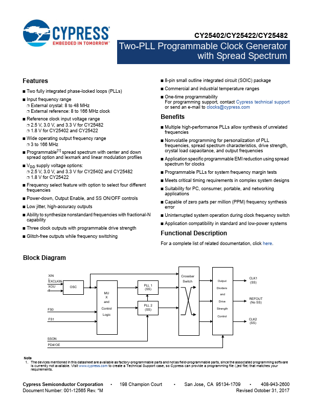
- Two fully integrated phase-locked loops (PLLs)
- Input frequency range
- External crystal: 8 to 48 MHz
- External reference: 8 to 166 MHz clock
- Reference clock input voltage range
- 2.5 V, 3.0 V, and 3.3 V for CY25482
- 1.8 V for CY25402 and CY25422
- Wide operating output frequency range
- 3 to 166 MHz
- Programmable[1] spread spectrum with center and down spread option and lexmark and linear modulation profiles