Datasheet4U Logo Datasheet4U.com

CY7B9930V - (CY7B9930V / CY7B9940V) High Speed Multifrequency PLL Clock Buffer

General Description

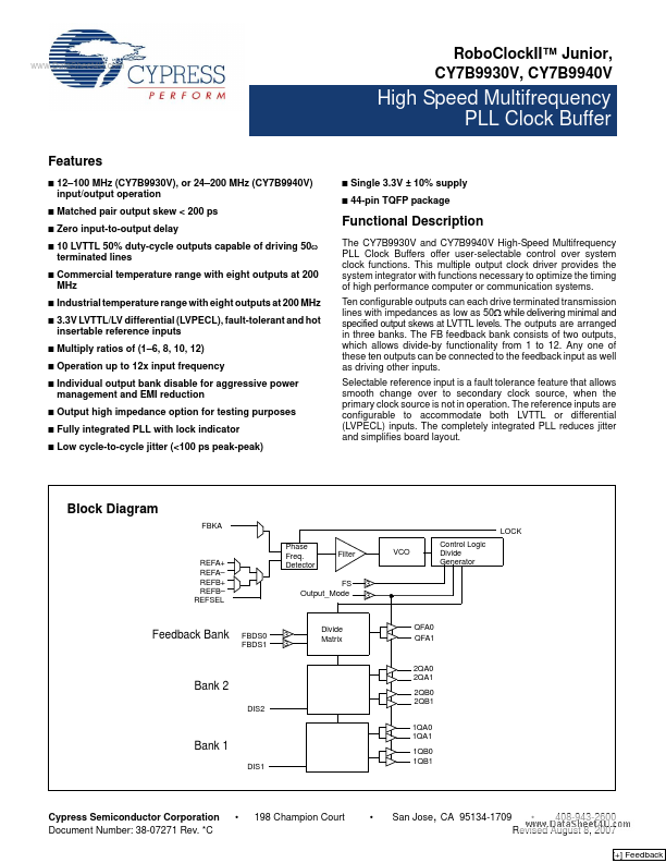
The CY7B9930V and CY7B9940V High-Speed Multifrequency PLL Clock Buffers offer user-selectable control over system clock functions.

This multiple output clock driver provides the system integrator with functions necessary to optimize the timing of high performance computer or communication systems.

Key Features

  • 12.
  • 100 MHz (CY7B9930V), or 24.
  • 200 MHz (CY7B9940V) input/output operation Matched pair output skew < 200 ps Zero input-to-output delay 10 LVTTL 50% duty-cycle outputs capable of driving 50ω terminated lines Commercial temperature range with eight outputs at 200 MHz Industrial temperature range with eight outputs at 200 MHz 3.3V LVTTL/LV differential (LVPECL), fault-tolerant and hot insertable reference.

📥 Download Datasheet

Full PDF Text Transcription for CY7B9930V (Reference)

Note: Below is a high-fidelity text extraction (approx. 800 characters) for CY7B9930V. For precise diagrams, and layout, please refer to the original PDF.

www.DataSheet4U.com RoboClockII™ Junior, CY7B9930V, CY7B9940V High Speed Multifrequency PLL Clock Buffer Features ■ ■ ■ ■ ■ ■ ■ ■ ■ ■ ■ ■ ■ 12–100 MHz (CY7B9930V), or 24–...

View more extracted text
ffer Features ■ ■ ■ ■ ■ ■ ■ ■ ■ ■ ■ ■ ■ 12–100 MHz (CY7B9930V), or 24–200 MHz (CY7B9940V) input/output operation Matched pair output skew < 200 ps Zero input-to-output delay 10 LVTTL 50% duty-cycle outputs capable of driving 50ω terminated lines Commercial temperature range with eight outputs at 200 MHz Industrial temperature range with eight outputs at 200 MHz 3.