Datasheet Summary
PLEMENTARY PAIR ENHANCEMENT MODE MOSFET
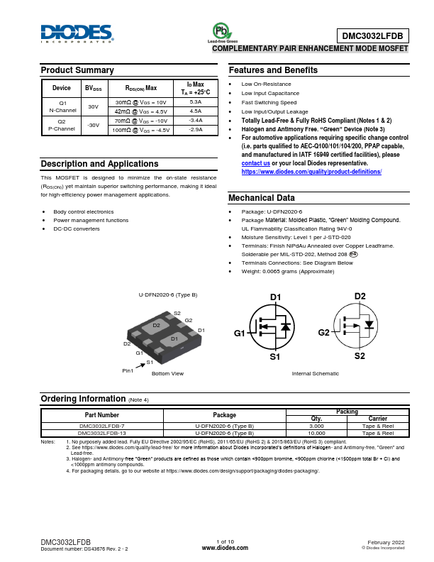
Product Summary
Device
BVDSS
Q1 N-Channel
Q2 P-Channel
30V -30V
RDS(ON) Max
30mΩ @ VGS = 10V 42mΩ @ VGS = 4.5V 70mΩ @ VGS = -10V 100mΩ @ VGS = -4.5V
ID Max TA = +25°C
5.3A 4.5A -3.4A -2.9A
Description and Applications
This MOSFET is designed to minimize the on-state resistance (RDS(ON)) yet maintain superior switching performance, making it ideal for high-efficiency power management applications.
- Body control electronics
- Power management functions
- DC-DC converters
Features and Benefits
- Low On-Resistance
- Low Input Capacitance
- Fast Switching Speed
- Low Input/Output Leakage
- Totally Lead-Free & Fully RoHS pliant...