PI6C39X0202 Overview
Description
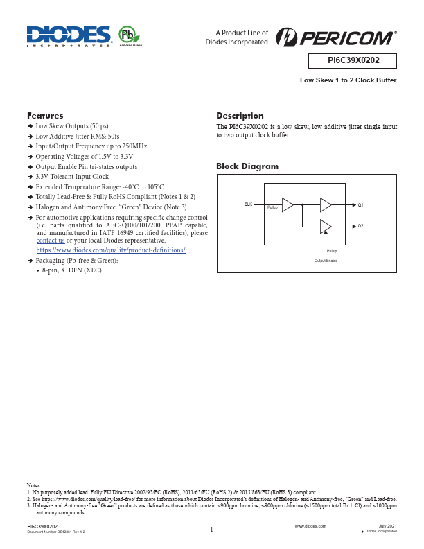
The PI6C39X0202 is a low skew, low additive jitter single input to two output clock buffer. CLK Pullup Q1 Q2 Pullup Output Enable Notes: 1.
Key Features
- Î Halogen and Antimony Free. “Green” Device (Note
| Part | PI6C39X0202 |
|---|---|
| Description | Low Skew 1 to 2 Clock Buffer |
| Manufacturer | Diodes Incorporated |
| Size | 819.24 KB |
The PI6C39X0202 is a low skew, low additive jitter single input to two output clock buffer. CLK Pullup Q1 Q2 Pullup Output Enable Notes: 1.
| Part Number | Manufacturer | Description |
|---|---|---|
| BUF04 | Analog Devices | Closed-Loop High Speed Buffer |
| 74HC125 | NXP Semiconductors | Quad buffer/line driver |
| BUF03 | Analog Devices | High Speed Voltage Follower/Buffer |