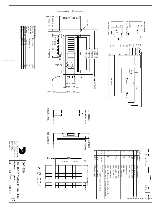
Pin 1 2 3 VSS VDD VEE
Symbol
Signal Description
Logic Ground (0V)
Power Supply (5V)
LCD Drive Voltage
Register Select 4 RS
High = Data
Low = Instruction
Signal Description 5 R/W
High = LCM to MPU
Low = MPU to LCM
Signal Description 6 E
R/W = Low;Data read at falling edge of E
R/W = Hig
Full PDF Text Transcription for DV16244 (Reference)
Note: Below is a high-fidelity text extraction (approx. 800 characters) for
DV16244. For precise diagrams, and layout, please refer to the original PDF.
Block Diagram VDD +5V 10k E Controler LSI LCD Panel COM 8 SEG 40 SEG 40 R/W VSS RS VEE VDD +5V VSS Standard Temp Display VDD VSS VEE -5V LED A LED Backlight LED K Extende...
View more extracted text
tandard Temp Display VDD VSS VEE -5V LED A LED Backlight LED K Extended Temp Display 10k COM 8 VEE DB0 ~ DB7 1 New Release 8/17/01 Pin Description Pin 1 2 3 VSS VDD VEE Symbol Signal Description Logic Ground (0V) Power Supply (5V) LCD Drive Voltage Register Select 4 RS High = Data Low = Instruction Signal Description 5 R/W High = LCM to MPU Low = MPU to LCM Signal Description 6 E R/W = Low;Data read at falling edge of E R/W = High; Data can be read when E is high 7~14 DB0~DB7 15 LED K 16 LED A Data Bus 4 or 8 bit parallel, software selectable 84.00 [3.31] 79.00 [3.11] 2.50 [0.10] 71.20 [2.80] 2-R1.25 56.20 [2.21] 62.20 [2.