FEATURES
● TrenchFET® Power MOSFET
● 100 % Rg and UIS Tested
● Material categorization: APPLICATIONS
● DC/DC Converters / Boost Converters
● Load Switch
● LED Backlighting in LCD TVs
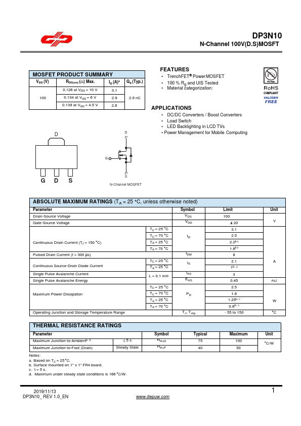
● Power Management for Mobile Computing G GD S S N-Channel MOSFET ABSOLUTE MAXIMUM RATINGS
(TA = 25 °C, unless otherwise noted) Parameter Drain-Source Voltage Gate-Source Voltage Continuous Drain Current (TJ = 150 °C) Pulsed Drain Current (t = 300 µs) Continuous Source-Drain Diode Current Single Pulse Avalanche Current Single Pulse Avalanche Energy Maximum Power Dissipation Operating Junction and Storage Temperature Range TC = 25 °C TC = 70 °C TA = 25 °C TA = 70 °C TC = 25 °C TA = 25 °C L = 0.1 mH TC = 25 °C TC = 70 °C TA = 25 °C TA = 70 °C Symbol VDS VGS ID IDM IS IAS EAS PD TJ, Tstg THERMAL RESISTANCE RATINGS Parameter Maximum Junction-to-Ambientb, d Maximum Junction-to-Foot (Drain) ≤5s Steady State Notes: a. Based on TC = 25 °C. b. Surface mounted on 1" x 1" FR4 board. c. t = 5 s. d. Maximum under steady state conditions is 166 °C/W.