Datasheet Summary
NOT REMENDED FOR NEW DESIGN USE DMT6016LPS
50V N-CHANNEL MOSFET
Description
This N-Channel MOSFET has been designed specifically to improve the overall efficiency and to minimize switch node ringing of DC-DC converters using either synchronous or conventional switching PWM controllers. It has been optimized for low gate charge, low RDS(ON), fast switching speed and body diode reverse recovery performance.
The AF15N50 is available in PDFN-5×6-8 package.
Features
- Typ RDS(ON)=14.32mΩ @ VGS=10V, ID=15A
- Typ RDS(ON)=16.36mΩ @ VGS=4.5V, ID=15A
- RoHS pliant
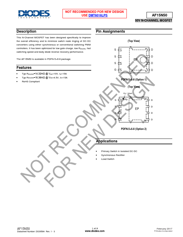
Pin Assignments
(Top View)
S1 S2 S3 G4
8D
7D
6D
5D
PDFN-5×6-8 (Option 1) (Top View)
Pin 1 Mark
S1
8D
S2 S3...