DMP4015SK3 Description
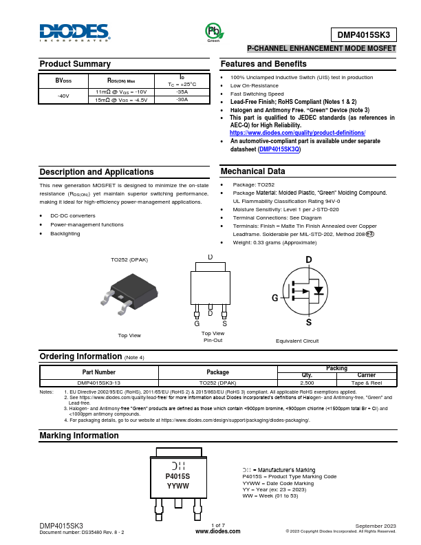
and Applications This new generation MOSFET is designed to minimize the on-state resistance (RDS(ON)) yet maintain superior switching performance, making it ideal for high-efficiency power-management applications. DC-DC converters Power-management functions Backlighting Package: TO252 Package Material:.
DMP4015SK3 Key Features
- 100% Unclamped Inductive Switch (UIS) test in production
- Low On-Resistance
- Fast Switching Speed
- Lead-Free Finish; RoHS pliant (Notes 1 & 2)
- Halogen and Antimony Free. “Green” Device (Note 3)
- An automotive-pliant part is available under separate datasheet (DMP4015SK3Q)