Datasheet4U Logo Datasheet4U.com

PI6C5921512 Datasheet 12 Output LVDS Fanout Buffer

Manufacturer: Diodes Incorporated

General Description

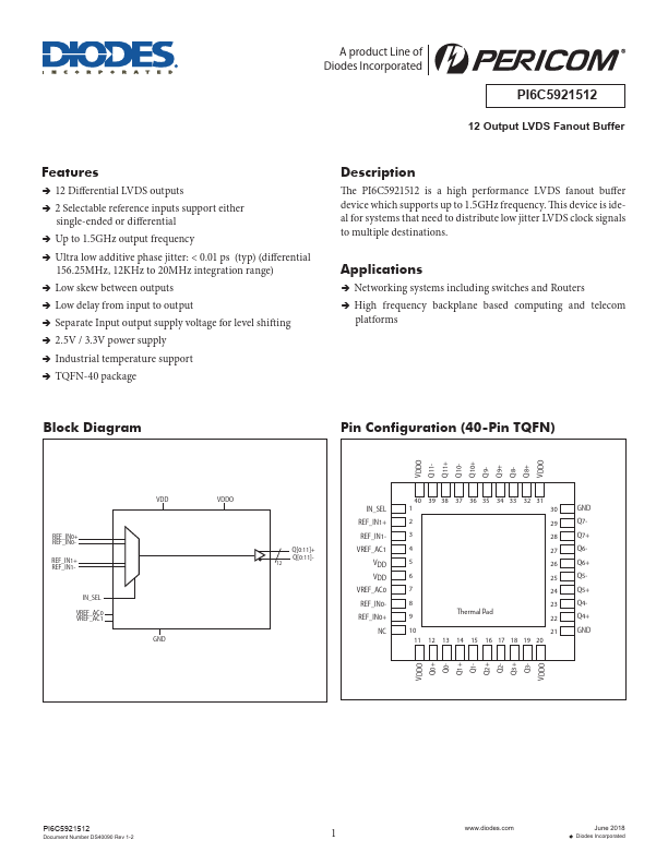
The PI6C5921512 is a high performance LVDS fanout buffer device which supports up to 1.5GHz frequency.

This device is ideal for systems that need to distribute low jitter LVDS clock signals to multiple destinations.

Applications ÎÎNetworking systems including switches and Routers ÎÎHigh frequency backplane based computing and telecom platforms Block Diagram Pin Configuration (40-Pin TQFN) VDDO Q11Q11+ Q10Q10+ Q9Q9+ Q8Q8+ VDDO REF_IN0+ REF_IN0REF_IN1+ REF_IN1- IN_SEL VREF_AC0 VREF_AC1 VDD GND VDDO Q[0:11]+ Q[0:11]12 IN_SEL REF_IN1+ REF_IN1VREF_AC1 VDD VDD VREF_AC0 REF_IN0REF_IN0+ NC 40 39 38 37 36 35 34 33 32 31 1 30 2 29 3 28 4 27 5 26 6 25 7 24 8 9 Thermal Pad 23 22 10 21 11 12 13 14 15 16 17 18 19 20 GND Q7Q7+ Q6Q6+ Q5Q5+ Q4Q4+ GND VDDO Q0+ Q0Q1+ Q1Q2+ Q2Q3+ Q3- VDDO PI6C5921512 Document Number DS40090 Rev 1-2 1 www.diodes.com June 2018 Diodes Incorporated Pin Description Pin # Pin Name 1 IN_SEL 2,3 REF_IN1+ REF_IN1- 4 VREF_AC1 5, 6 7 8, 9 10 11, 20, 31, 40 12, 13 14, 15 16, 17 18, 19 21, 30 22, 23 24, 25 26, 27 28, 29 32, 33 34, 35 36, 37 VDD VREF_AC0 REF_IN0REF_IN0+ NC VDDO Q0+ Q0Q1+ Q1Q2+ Q2Q3+ Q3GND Q4+ Q4Q5+ Q5Q6+ Q6Q7+ Q7Q8+ Q8- Q9+ Q9Q10+ Q10- PI6C5921512 Document Number DS40090 Rev 1-2 A product Line of Diodes Incorporated PI6C5921512 Type Description Input Pulldown Input clock select.

Overview

A product Line of Diodes Incorporated PI6C5921512 12 Output LVDS Fanout.

Key Features

  • ÎÎ12 Differential LVDS outputs ÎÎ2 Selectable reference inputs support either single-ended or differential ÎÎUp to 1.5GHz output frequency ÎÎUltra low additive phase jitter: < 0.01 ps (typ) (differential 156.25MHz, 12KHz to 20MHz integration range) ÎÎLow skew between outputs ÎÎLow delay from input to output ÎÎSeparate Input output supply voltage for level shifting ÎÎ2.5V / 3.3V power supply ÎÎIndustrial temperature support ÎÎTQFN-40 package.