ZXCT1109SA-7
ZXCT1109SA-7 is LOW POWER HIGH-SIDE CURRENT MONITORS manufactured by Diodes Incorporated.
- Part of the ZXCT1107 comparator family.
- Part of the ZXCT1107 comparator family.
Description
The ZXCT1107/09/10 are high side unipolar current sense monitors. These devices eliminate the need to disrupt the ground plane when sensing a load current.
The wide mon-mode input voltage range and low quiescent current coupled with SOT23 packages make them suitable for a range of applications; including adapters, automotive and systems operating from industrial 24V rails.
The device is line powered and as such doesn’t need a separate supply rail.
Quiescent current is only 3µA thereby minimising current sensing error. One external gain setting resistor increases versatility by permitting wide gain ranges.
Features
- Wide supply and mon-mode voltage range: 2.5V to 36V
- SOT23 packages o 3-pin ZXCT1107/09 o 5-pin ZXCT1110
- Low quiescent current (3µA).
- Extended industrial temperature range -40 to 125°C
- AEC-Q100 Grade1 Automotive qualified variants
Applications
- Automotive current measurement
- Industrial applications current measurement
- Battery management
- Over current monitor
- Power Management
Typical Application Circuit
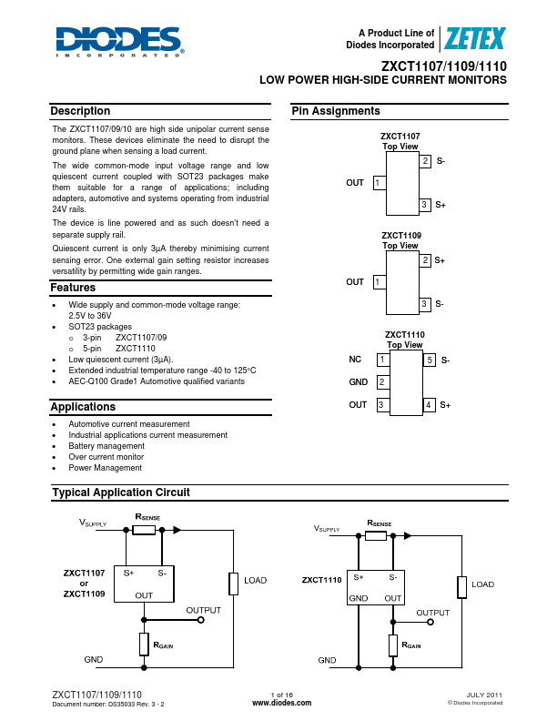
Pin Assignments
ZXCT1107 Top View
2 S-
OUT 1
3 S+
ZXCT1109 Top View
2 S+
OUT 1
3 S-
ZXCT1110 Top View
NC 1
5 S-
GND 2
OUT 3
4 S+
ZXCT1107/1109/1110
Document number: DS35033 Rev. 3
- 2
1 of 16 .diodes.
JULY 2011
© Diodes Incorporated
NEW...