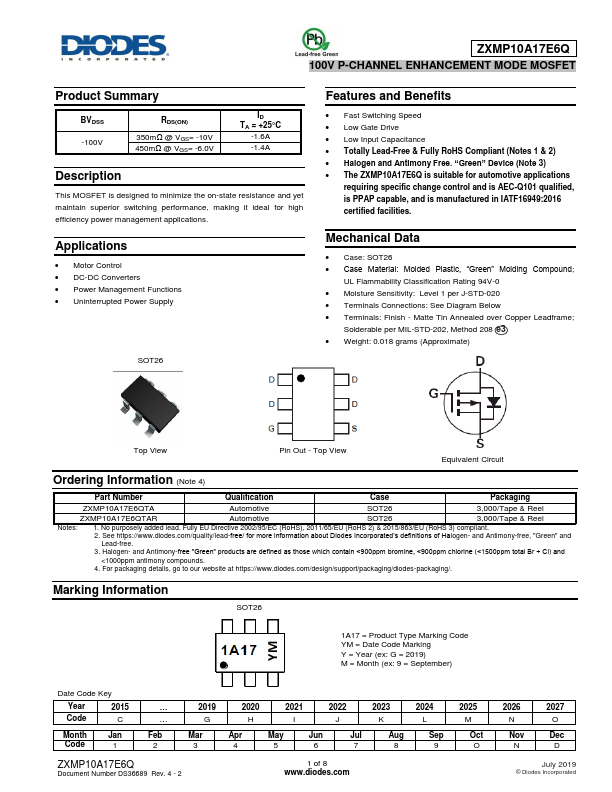
ZXMP10A17E6Q Description
This MOSFET is designed to minimize the on-state resistance and yet maintain superior switching performance, making it ideal for high efficiency power management applications. Applications Motor Control DC-DC Converters Power Management Functions Uninterrupted Power Supply SOT26.
ZXMP10A17E6Q Key Features
- Fast Switching Speed
- Low Gate Drive
- Low Input Capacitance
- Totally Lead-Free & Fully RoHS pliant (Notes 1 & 2)
- Halogen and Antimony Free. “Green” Device (Note 3)
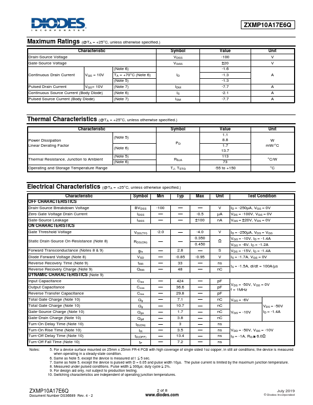
- The ZXMP10A17E6Q is suitable for automotive