ETA3412
ETA3412 is Dual 1.5MHz 1.2A Step-Down Converters manufactured by ETA.
DESCRIPTION
The ETA3412 is a dual channel high-efficiency, DC-to-DC step-down switching regulator, capable of delivering up to 1.2A of output current for each channel. The devices operate from an input voltage range of 2.6V to 6V and provide output voltages from 0.6V to VIN, making the ETA3412 ideal for low voltage power conversions. Running at a fixed frequency of 1.5MHz allows the use of small inductance value and low DCR inductors, thereby achieving higher efficiencies. Other external ponents, such as ceramic input and output caps, can also be small due to higher switching frequency, while maintaining exceptional low noise output voltages. Built-in EMI reduction circuitry makes this converter ideal power supply for RF applications. Internal soft-start control circuitry reduces inrush current. Short-circuit and thermal-overload protection improves design reliability. ETA3412 is housed in a SOP8 package
FEATURES
- Up to 1.2A Max Output Current
- 1.5MHz Frequency
- Light Load operation
- Internal pensation
- Available in SOP8
APPLICATIONS
- USB ports/Hubs
- Hot Swaps
- Cellphones
- Tablet PC
- Set Top Boxes
ORDERING INFORMATION
PART PACKAGE PIN ETA3412S8A SOP8
TOP MARK
ETA3412-Product Number YWWPL-Date Code
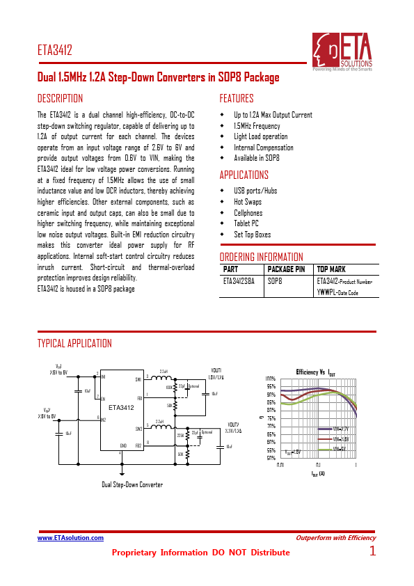
TYPICAL APPLICATION
VIN1 2.6V to 6V
VIN2 2.6V to 6V
10u F
2 IN1 SW1 3
10u F 7 EN
1 FB1
2.2u H 100K 22p F Optional 50K
VOUT1 1.8V/1.2A
10u F
6 IN2
SW2 5 2.2u H
225K 22p F Optional
VOUT2 3.3V/1.2A
GND FB2 8
10u F
4 50K
Dual Step-Down Converter
ŋ
100% Efficiency Vs...