logo
Datasheet4U.com - BD4833G
logo

BD4833G Datasheet, RESET, ETC

BD4833G Datasheet, RESET, ETC

BD4833G

datasheet Download (Size : 219.48KB)

BD4833G Datasheet
BD4833G

datasheet Download (Size : 219.48KB)

BD4833G Datasheet

BD4833G Features and benefits

BD4833G Features and benefits

1) Detection voltage: 0.1V step line-up 2.3~6.0V (Typ.) 2) High-accuracy detection voltage:±1.5% Max. 3) Ultra low current consumption: 0.8µA typ. 4) Nch open drain outpu.

BD4833G Application

BD4833G Application

Every kind of appliances with microcontroller and logic circuit Application Circuit BD48XXG/FVE VDD VDD VDD VDD BD48XXF.

BD4833G Description

BD4833G Description

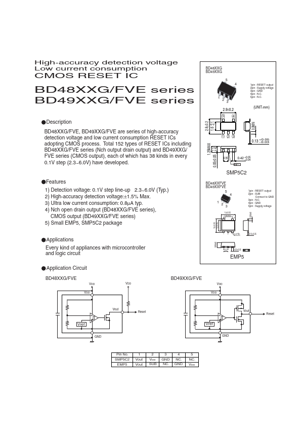
Reset Vref Vref GND GND Pin No. SMP5C2 EMP5 1 Vout Vout 2 VDD SUB 3 GND NC. 4 NC. GND 5 NC. VDD http://www.Datasheet4U.com Absolute Maximum Ratings (Ta=25˚C) Parameter Power supply voltage CMOS output Power dissipation (SMP5C2) ∗1 Power .

Image gallery

BD4833G Page 1 BD4833G Page 2 BD4833G Page 3

TAGS

BD4833G
CMOS
RESET
ETC

Manufacturer


ETC

Related datasheet

BD4833

BD4833FVE

BD4830

BD4830FVE

BD4830G

BD4831

BD4831FVE

BD4831G

BD4832

BD4832FVE

Since 2006. D4U Semicon.   |   Datasheet4U.com   |   Contact Us   |   Privacy Policy   |   Purchase of parts