Datasheet4U Logo Datasheet4U.com

TM50S116T - SDRAM

Description

The TM50S116T is organized as 2-bank x 524288-word x 16-bit(1Mx16), fabricated with high performance CMOS technology.

Synchronous design allows precise cycle control with the use of system clock I/O transactions are possible on every clock cycle.

Features

  • n Package 400-mil 50-pin TSOP(II) n JEDEC PC133/PC100 compatible n Single 3.3V Power Supply n LVTTL Signal Compatible n Byte control(DQML and DQMU) n Auto and Self Refresh n 64ms refresh period (4K cycles) n 11-Row x 8-Column organization n 2-Bank operation controlled by BA0 n Programmable n Pin33 and 37 are “No Connected” - CAS Latency (3 or 2 clocks) n Fully synchronous operation referenced - Burst Length (1,2,4,8 & full page) to clock rising edge - Burst type (Sequential & Interleave) n Burst.

📥 Download Datasheet

Datasheet Details

Part number TM50S116T
Manufacturer Unknown Manufacturer
File Size 93.32 KB
Description SDRAM
Datasheet download datasheet TM50S116T Datasheet

Full PDF Text Transcription (Reference)

The following content is an automatically extracted verbatim text from the original manufacturer datasheet and is provided for reference purposes only.

View original datasheet text
TMC Description TM50S116T SDRAM The TM50S116T is organized as 2-bank x 524288-word x 16-bit(1Mx16), fabricated with high performance CMOS technology. Synchronous design allows precise cycle control with the use of system clock I/O transactions are possible on every clock cycle. Range of operating frequencies, programmable burst length and programmable latencies allow the same device to be useful for a variety of high bandwidth, high performance memory system applications. 
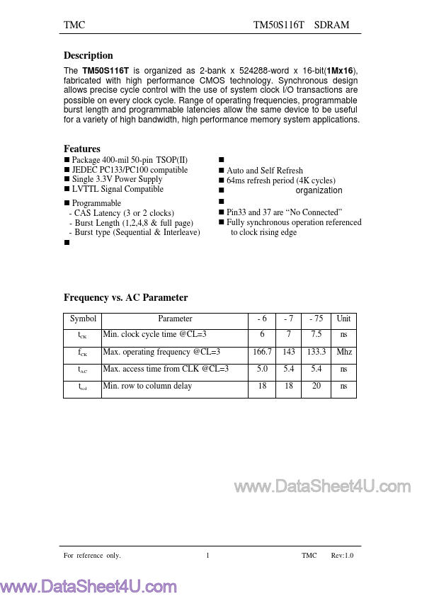
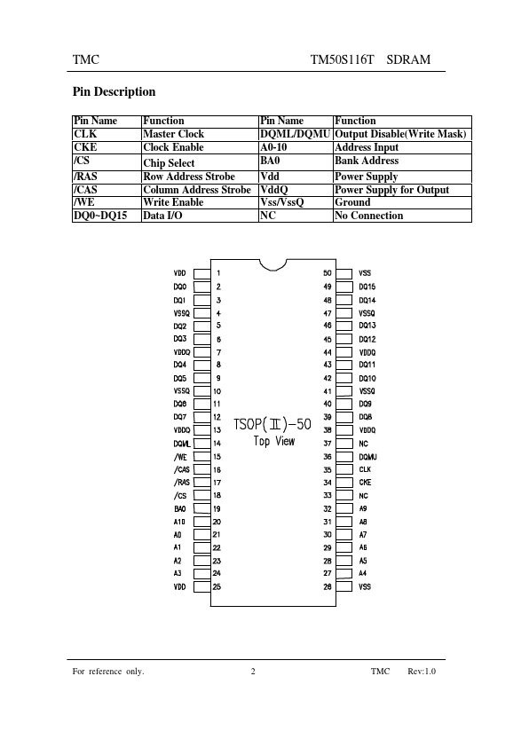
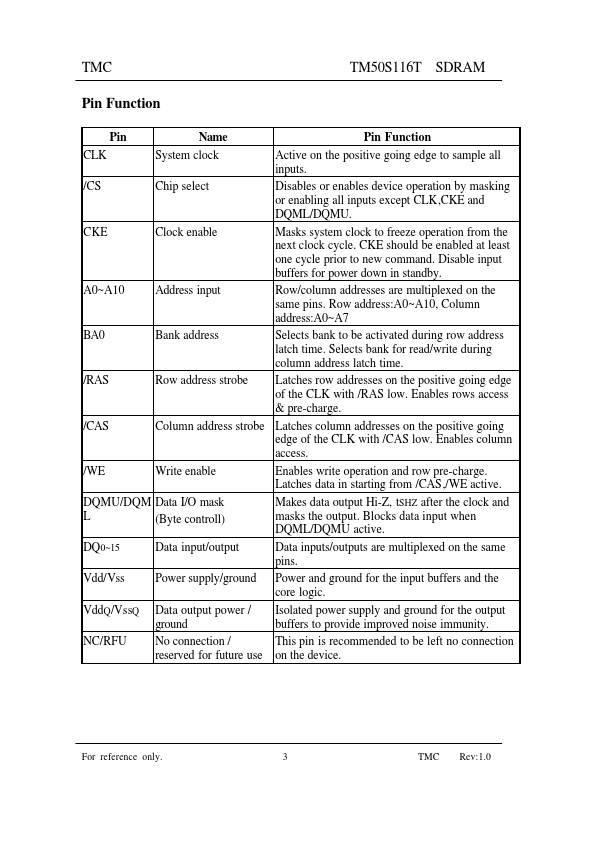
Features n Package 400-mil 50-pin TSOP(II) n JEDEC PC133/PC100 compatible n Single 3.
Published: |