Datasheet4U Logo Datasheet4U.com

EDJ2116DEBG Datasheet 2G bits DDR3 SDRAM

Manufacturer: Elpida Memory

Download the EDJ2116DEBG datasheet PDF. This datasheet also includes the EDJ2108DEBG variant, as both parts are published together in a single manufacturer document.

📥 Download Datasheet

Note: The manufacturer provides a single datasheet file (EDJ2108DEBG-ElpidaMemory.pdf) that lists specifications for multiple related part numbers.

Datasheet Details

Part number EDJ2116DEBG
Manufacturer Elpida Memory
File Size 297.00 KB
Description 2G bits DDR3 SDRAM
Download EDJ2116DEBG Download (PDF)

Overview

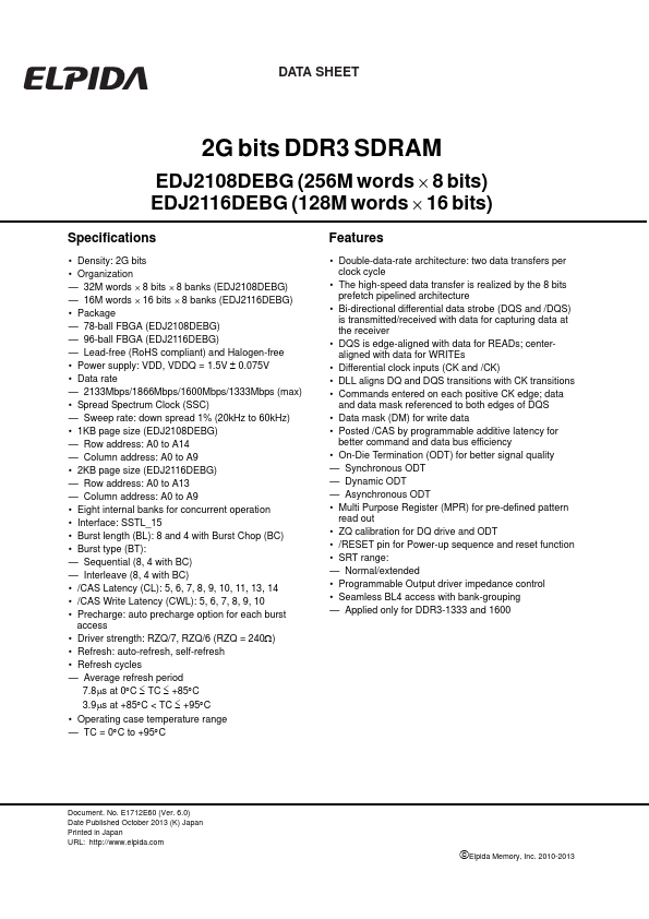
COVER DATA SHEET 2G bits DDR3 SDRAM EDJ2108DEBG (256M words × 8 bits) EDJ2116DEBG (128M words × 16 bits) Specifications • Density: 2G bits • Organization — 32M words × 8 bits × 8 banks (EDJ2108DEBG) — 16M words × 16 bits × 8 banks (EDJ2116DEBG) • Package — 78-ball FBGA (EDJ2108DEBG) — 96-ball FBGA (EDJ2116DEBG) — Lead-free (RoHS compliant) and Halogen-free • Power supply: VDD, VDDQ = 1.5V ± 0.075V • Data rate — 2133Mbps/1866Mbps/1600Mbps/1333Mbps (max) • Spread Spectrum Clock (SSC) — Sweep rate: down spread 1% (20kHz to 60kHz) • 1KB page size (EDJ2108DEBG) — Row address: A0 to A14 — Column address: A0 to A9 • 2KB page size (EDJ2116DEBG) — Row address: A0 to A13 — Column address: A0 to A9 • Eight internal banks for concurrent operation • Interface: SSTL_15 • Burst length (BL): 8 and 4 with Burst Chop (BC) • Burst type (BT): — Sequential (8, 4 with BC) — Interleave (8, 4 with BC) • /CAS Latency (CL): 5, 6, 7, 8, 9, 10, 11, 13, 14 • /CAS Write Latency (CWL): 5, 6, 7, 8, 9, 10 • Precharge: auto precharge option for each burst access • Driver strength: RZQ/7, RZQ/6 (RZQ = 240Ω) • Refresh: auto-refresh, self-refresh • Refresh cycles — Average refresh period 7.8µs at 0°C ≤ TC ≤ +85°C 3.

Key Features

  • Double-data-rate architecture: two data transfers per clock cycle.
  • The high-speed data transfer is realized by the 8 bits prefetch pipelined architecture.
  • Bi-directional differential data strobe (DQS and /DQS) is transmitted/received with data for capturing data at the receiver.
  • DQS is edge-aligned with data for READs; centeraligned with data for WRITEs.
  • Differential clock inputs (CK and /CK).
  • DLL aligns DQ and DQS transitions with CK transi.