Datasheet4U Logo Datasheet4U.com

EDJ4208EFBG Datasheet 512M words x 8 bits 4G bits DDR3L SDRAM

Manufacturer: Elpida Memory

Download the EDJ4208EFBG datasheet PDF. This datasheet also includes the EDJ4204EFBG variant, as both parts are published together in a single manufacturer document.

📥 Download Datasheet

Note: The manufacturer provides a single datasheet file (EDJ4204EFBG-ElpidaMemory.pdf) that lists specifications for multiple related part numbers.

Datasheet Details

Part number EDJ4208EFBG
Manufacturer Elpida Memory
File Size 392.78 KB
Description 512M words x 8 bits 4G bits DDR3L SDRAM
Datasheet download datasheet EDJ4208EFBG Datasheet

Overview

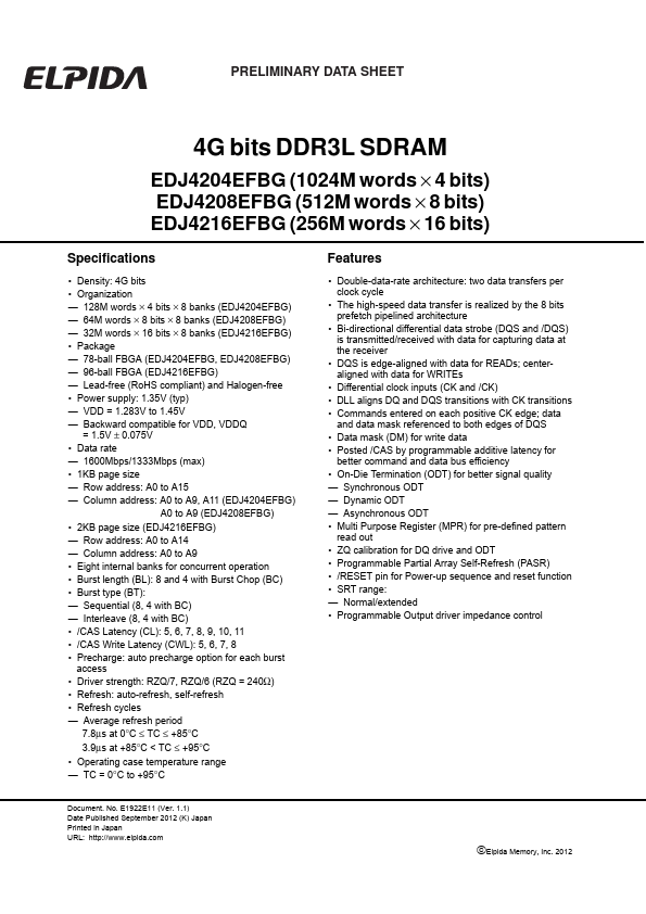
COVER PRELIMINARY DATA SHEET 4G bits DDR3L SDRAM EDJ4204EFBG (1024M words × 4 bits) EDJ4208EFBG (512M words × 8 bits) EDJ4216EFBG (256M words × 16 bits) Specifications • Density: 4G bits • Organization — 128M words × 4 bits × 8 banks (EDJ4204EFBG) — 64M words × 8 bits × 8 banks (EDJ4208EFBG) — 32M words × 16 bits × 8 banks (EDJ4216EFBG) • Package — 78-ball FBGA (EDJ4204EFBG, EDJ4208EFBG) — 96-ball FBGA (EDJ4216EFBG) — Lead-free (RoHS compliant) and Halogen-free • Power supply: 1.35V (typ) — VDD = 1.283V to 1.45V — Backward compatible for VDD, VDDQ = 1.5V ± 0.075V • Data rate — 1600Mbps/1333Mbps (max) • 1KB page size — Row address: A0 to A15 — Column address: A0 to A9, A11 (EDJ4204EFBG) A0 to A9 (EDJ4208EFBG) • 2KB page size (EDJ4216EFBG) — Row address: A0 to A14 — Column address: A0 to A9 • Eight internal banks for concurrent operation • Burst length (BL): 8 and 4 with Burst Chop (BC) • Burst type (BT): — Sequential (8, 4 with BC) — Interleave (8, 4 with BC) • /CAS Latency (CL): 5, 6, 7, 8, 9, 10, 11 • /CAS Write Latency (CWL): 5, 6, 7, 8 • Precharge: auto precharge option for each burst access • Driver strength: RZQ/7, RZQ/6 (RZQ = 240Ω) • Refresh: auto-refresh, self-refresh • Refresh cycles — Average refresh period 7.8µs at 0°C ≤ TC ≤ +85°C 3.

Key Features

  • Double-data-rate architecture: two data transfers per clock cycle.
  • The high-speed data transfer is realized by the 8 bits prefetch pipelined architecture.
  • Bi-directional differential data strobe (DQS and /DQS) is transmitted/received with data for capturing data at the receiver.
  • DQS is edge-aligned with data for READs; centeraligned with data for WRITEs.
  • Differential clock inputs (CK and /CK).
  • DLL aligns DQ and DQS transitions with CK transi.