EM566169BC Description
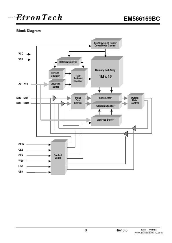
It is designed with advanced CMOS technology specified RAM featuring low power static RAM patible function and . This device operates from a single power supply. Advanced circuit technology provides both high speed and low power.
EM566169BC Key Features
- Organized as 1M words by 16 bits
- Fast Cycle Time : 60/65/70/85ns
- Fast Page Cycle Time : 18/20/25/30ns
- Page Read Operation by 8 words
- Standby Current(ISB1): 100uA
- Deep power-down Current : 10uA (Memory cell data invalid)
- Byte data control: LB# (DQ0
- 7), UB# (DQ8
- patible with low power SRAM
- Single Power Supply Voltage : 3.0V±0.3V