The following content is an automatically extracted verbatim text
from the original manufacturer datasheet and is provided for reference purposes only.
View original datasheet text
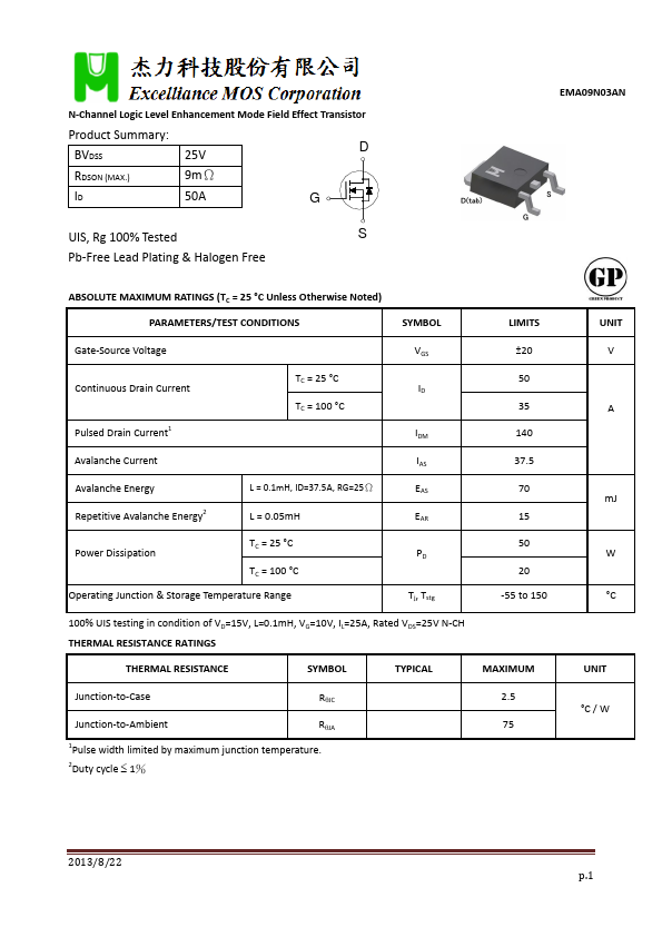
N‐Channel Logic Level Enhancement Mode Field Effect Transistor
Product Summary:
BVDSS
25V
D
RDSON (MAX.)
9mΩ
ID 50A G
UIS, Rg 100% Tested
S
Pb‐Free Lead Plating & Halogen Free
ABSOLUTE MAXIMUM RATINGS (TC = 25 °C Unless Otherwise Noted)
PARAMETERS/TEST CONDITIONS
SYMBOL
EMA09N03AN
LIMITS
UNIT
Gate‐Source Voltage
Continuous Drain Current Pulsed Drain Current1
TC = 25 °C TC = 100 °C
Avalanche Current
Avalanche Energy
L = 0.1mH, ID=37.5A, RG=25Ω
Repetitive Avalanche Energy2
L = 0.05mH
Power Dissipation
TC = 25 °C TC = 100 °C
Operating Junction & Storage Temperature Range
VGS ID
IDM IAS EAS EAR PD
Tj, Tstg
±20 50 35 140 37.5 70 15 50 20 ‐55 to 150
V A
mJ W °C
100% UIS testing in condition of VD=15V, L=0.
 EMA09N03AN Datasheet