EMB32N03J Description
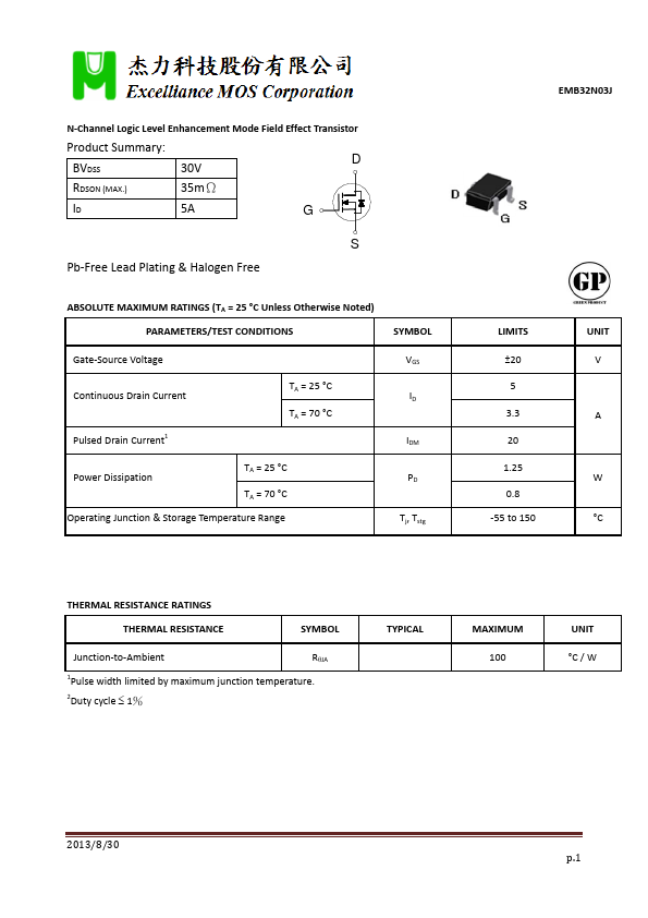
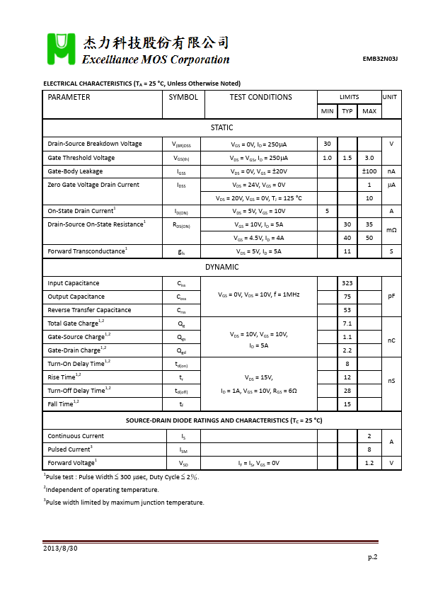
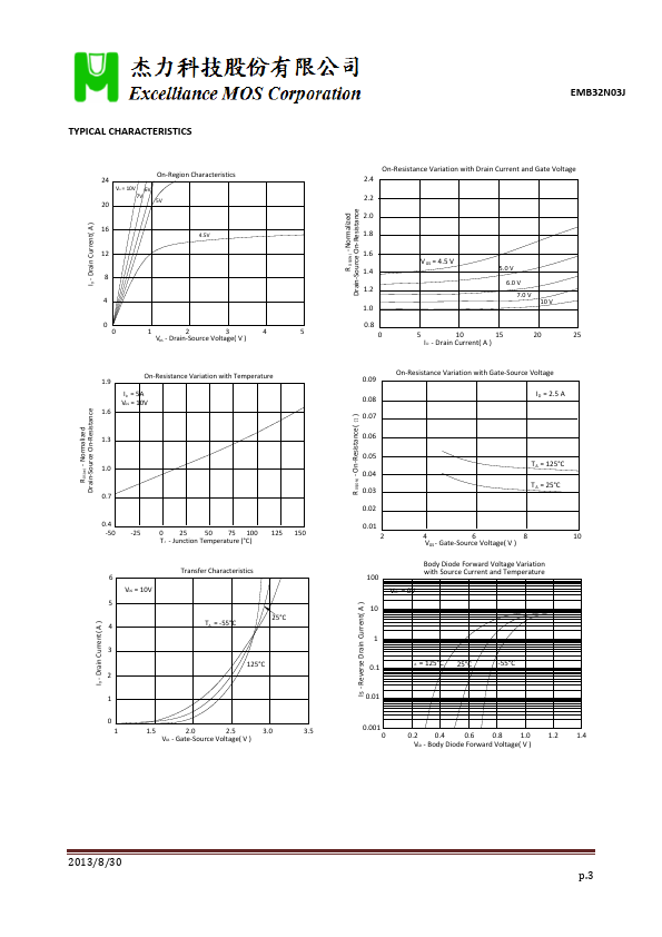
N‐Channel Logic Level Enhancement Mode Field Effect Transistor Product Summary: Pulse Width 300 sec, Duty Cycle 2%. 2Independent of operating temperature.
EMB32N03J is MOSFET manufactured by Excelliance MOS.
| Part Number | Description |
|---|---|
| EMB32N03JS | N-Channel Logic Level Enhancement Mode Field Effect Transistor |
| EMB32N03K | N-Channel MOSFET |
| EMB32N03P | MOSFET |
| EMB32N03VAT | MOSFET |
| EMB32A03G | Dual N-Channel Logic Level Enhancement Mode Field Effect Transistor |
N‐Channel Logic Level Enhancement Mode Field Effect Transistor Product Summary: Pulse Width 300 sec, Duty Cycle 2%. 2Independent of operating temperature.