74F219
74F219 is 64-Bit Random Access Memory manufactured by Fairchild Semiconductor.
74F219 64-Bit Random Access Memory with 3-STATE Outputs
June 1988 Revised July 1999
74F219 64-Bit Random Access Memory with 3-STATE Outputs
General Description
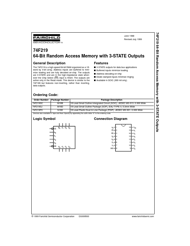
The 74F219 is a high-speed 64-bit RAM organized as a 16word by 4-bit array. Address inputs are buffered to minimize loading and are fully decoded on-chip. The outputs are 3-STATE and are in the high-impedance state whenever the Chip Select (CS) input is HIGH. The outputs are active only in the Read mode. This device is similar to the 74F189 but Features non-inverting, rather than inverting, data outputs.
Features s 3-STATE outputs for data bus applications s Buffered inputs minimize loading s Address decoding on-chip s Diode clamped inputs minimize ringing s Available in SOIC (300 mil only)
Ordering Code:
Order Number 74F219SC 74F219SJ 74F219PC Package Number M16B M16D N16E Package Description 16-Lead Small Outline Intergrated Circuit (SOIC), JEDEC MS-013, 0.300 Wide 16-Lead Small Outline Package (SOP), EIAJ TYPE II, 5.3mm Wide 16-Lead Plastic Dual-In-Line Package (PDIP), JEDEC MS-001, 0.300 Wide
Devices also available in Tape and Reel. Specify by appending the suffix letter “X” to the ordering code.
Logic Symbol
Connection Diagram
© 1999 Fairchild Semiconductor Corporation
DS009500
.fairchildsemi.
Unit Loading/Fan Out
Pin Names A0- A3 CS WE D0- D3 O0- O3 Description Address Inputs Chip Select Input (Active LOW) Write Enable Input (Active LOW) Data Inputs 3-STATE Data Outputs U.L. HIGH/LOW 1.0/1.0 1.0/2.0 1.0/1.0 1.0/1.0 150/40 (33.3) Input IIH/IIL Output IOH/IOL 20 µA/- 0.6 m A 20 µA/- 1.2 m A 20 µA/- 0.6 m A 20 µA/- 0.6 m A
- 3 m A/24 m A (20 m A)
Function Table
Inputs Operation CS L L H
H = HIGH Voltage Level L = LOW Voltage Level X = Immaterial
Condition of Outputs High Impedance True Stored Data High Impedance
WE L H X Write Read Inhibit
Block Diagram
.fairchildsemi....