74F379
74F379 is Quad Parallel Register manufactured by Fairchild Semiconductor.
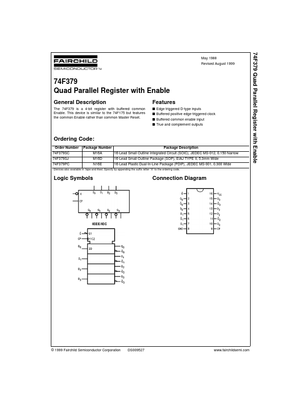
74F379 Quad Parallel Register with Enable
May 1988 Revised August 1999
74F379 Quad Parallel Register with Enable
General Description
The 74F379 is a 4-bit register with buffered mon Enable. This device is similar to the 74F175 but Features the mon Enable rather than mon Master Reset.
Features s Edge triggered D-type inputs s Buffered positive edge-triggered clock s Buffered mon enable input s True and plement outputs
Ordering Code:
Order Number 74F379SC 74F379SJ 74F379PC Package Number M16A M16D N16E Package Description 16-Lead Small Outline Integrated Circuit (SOIC), JEDEC MS-012, 0.150 Narrow 16-Lead Small Outline Package (SOP), EIAJ TYPE II, 5.3mm Wide 16-Lead Plastic Dual-In-Line Package (PDIP), JEDEC MS-001, 0.300 Wide
Devices also available in Tape and Reel. Specify by appending the suffix letter “X” to the ordering code.
Logic Symbols
Connection Diagram
IEEE/IEC
© 1999 Fairchild Semiconductor Corporation
DS009527
.fairchildsemi.
Unit Loading/Fan Out
U.L. Pin Names E D0- D3 CP Q0- Q3 Q0- Q3 Description HIGH/LOW Enable Input (Active LOW) Data Inputs Clock Pulse Input (Active Rising Edge) Flip-Flop Outputs plement Outputs 1.0/1.0 1.0/1.0 1.0/1.0 50/33.3 50/33.3 Input IIH/IIL Output IOH/IOL 20 µA/- 0.6 m A 20 µA/- 0.6 m A 20 µA/- 0.6 m A
- 1 m A/20 m A
- 1 m A/20 m A
Functional Description
The 74F379 consists of four edge-triggered D-type flipflops with individual D inputs and Q and Q outputs. The Clock (CP) and Enable (E) inputs are mon to all flipflops. When the E is input HIGH, the register will retain the present data independent of the CP input. The Dn and E inputs can change when the clock is in either state, provided that the remended setup and hold times are observed.
Truth Table
Inputs E H L L CP Outputs Dn X H L Qn NC H L Qn NC L H
H = HIGH Voltage Level L = LOW Voltage Level X = Immaterial = LOW-to-HIGH Transition NC = No Change
Logic Diagram
Please note that this diagram is provided only for the...