74ACT825
74ACT825 is 8-Bit D-Type Flip-Flop manufactured by Fairchild Semiconductor.
74ACT825 8-Bit D-Type Flip-Flop
July 1988 Revised September 2000
74ACT825 8-Bit D-Type Flip-Flop
General Description
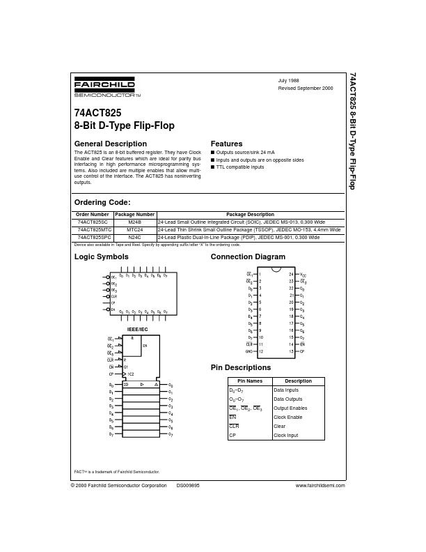
The ACT825 is an 8-bit buffered register. They have Clock Enable and Clear Features which are ideal for parity bus interfacing in high performance microprogramming systems. Also included are multiple enables that allow multiuse control of the interface. The ACT825 has noninverting outputs.
Features s Outputs source/sink 24 m A s Inputs and outputs are on opposite sides s TTL patible inputs
Ordering Code:
Order Number 74ACT825SC 74ACT825MTC 74ACT825SPC Package Number M24B MTC24 N24C Package Description 24-Lead Small Outline Integrated Circuit (SOIC), JEDEC MS-013, 0.300 Wide 24-Lead Thin Shrink Small Outline Package (TSSOP), JEDEC MO-153, 4.4mm Wide 24-Lead Plastic Dual-In-Line Package (PDIP), JEDEC MS-001, 0.300 Wide
Device also available in Tape and Reel. Specify by appending suffix letter “X” to the ordering code.
Logic Symbols
Connection Diagram
IEEE/IEC
Pin Descriptions
Pin Names D0- D7 O0- O7 OE1, OE2, OE3 EN CLR CP Description Data Inputs Data Outputs Output Enables Clock Enable Clear Clock Input
FACT is a trademark of Fairchild Semiconductor.
© 2000 Fairchild Semiconductor Corporation
DS009895
.fairchildsemi.
Functional Description
The ACT825 consists of eight D-type edge-triggered flipflops. These devices have 3-STATE outputs for bus systems, organized in a broadside pinning. In addition to the clock and output enable pins, the buffered clock (CP) and buffered Output Enable (OE) are mon to all flip-flops. The flip-flops will store the state of their individual D inputs that meet the setup and hold time requirements on the LOW-to-HIGH CP transition. With OE1, OE2 and OE3 LOW, the contents of the flip-flops are available at the outputs. When one of OE1, OE2 or OE3 is HIGH, the outputs go to the high impedance state. Operation of the OE input does not affect the state of the flip-flops. The ACT825 has Clear...