74LCXZ16240
74LCXZ16240 is Low Voltage 16-Bit Inverting Buffer/Line Driver manufactured by Fairchild Semiconductor.
Description
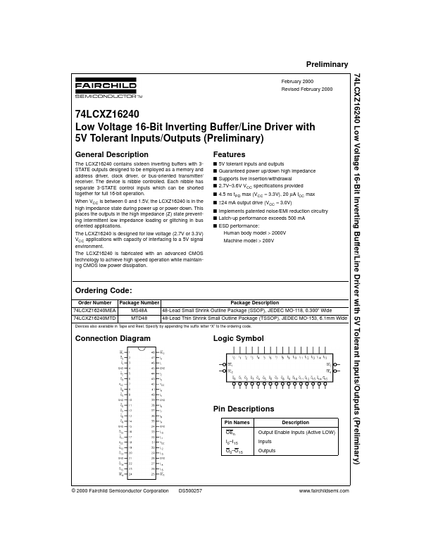
The LCXZ16240 contains sixteen inverting buffers with 3STATE outputs designed to be employed as a memory and address driver, clock driver, or bus-oriented transmitter/ receiver. The device is nibble controlled. Each nibble has separate 3-STATE control inputs which can be shorted together for full 16-bit operation. When VCC is between 0 and 1.5V, the LCXZ16240 is in the high impedance state during power up or power down. This places the outputs in the high impedance (Z) state preventing intermittent low impedance loading or glitching in bus oriented applications. The LCXZ16240 is designed for low voltage (2.7V or 3.3V) VCC applications with capacity of interfacing to a 5V signal environment. The LCXZ16240 is fabricated with an advanced CMOS technology to achieve high speed operation while maintaining CMOS low power dissipation.
Features s 5V tolerant inputs and outputs s Guaranteed power up/down high impedance s Supports live insertion/withdrawal s 2.7V- 3.6V VCC specifications provided s 4.5 ns t PD max (VCC = 3.3V), 20 µA ICC max s ±24 m A output drive (VCC = 3.0V) s Implements patented noise/EMI reduction circuitry s Latch-up performance exceeds 500 m A s ESD performance: Human body model > 2000V Machine model > 200V
Ordering Code:
Order Number 74LCXZ16240MEA 74LCXZ16240MTD Package Number MS48A MTD48 Package Description
48-Lead Small Shrink Outline Package (SSOP), JEDEC MO-118, 0.300” Wide 48-Lead Thin Shrink Small Outline Package (TSSOP), JEDEC MO-153, 6.1mm Wide
Devices also available in Tape and Reel. Specify by appending the suffix letter “X” to the ordering code.
Connection Diagram
Logic Symbol
Pin Descriptions
Pin Names OEn I0- I15 O0- O15 Description
Output Enable Inputs (Active LOW) Inputs Outputs
© 2000 Fairchild Semiconductor Corporation
DS500257
.fairchildsemi.
Preliminary 74LCXZ16240
Truth Tables
Inputs OE1 L L H I0- I3 L H X Outputs O0- O3 H L Z OE3 L L H Inputs I8- I11 L H X Outputs O8- O11 H L Z
Inputs OE2 L L H
H = HIGH Voltage Level...