• Part: 74VCX16721
  • Description: Low Voltage 20-Bit D-Type Flip-Flops with 3.6V Tolerant Inputs and Outputs
  • Manufacturer: Fairchild Semiconductor
  • Size: 85.32 KB
Download 74VCX16721 Datasheet PDF
Fairchild Semiconductor
74VCX16721
74VCX16721 is Low Voltage 20-Bit D-Type Flip-Flops with 3.6V Tolerant Inputs and Outputs manufactured by Fairchild Semiconductor.
Description 
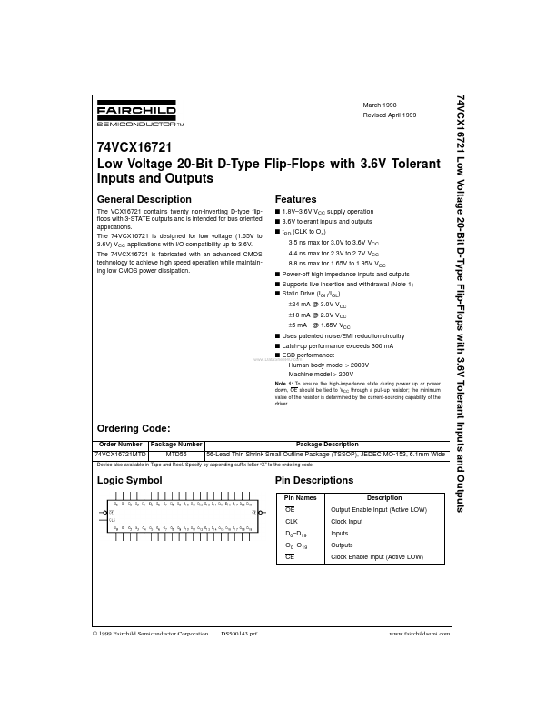
The VCX16721 contains twenty non-inverting D-type flipflops with 3-STATE outputs and is intended for bus oriented applications. The 74VCX16721 is designed for low voltage (1.65V to 3.6V) VCC applications with I/O patibility up to 3.6V. The 74VCX16721 is fabricated with an advanced CMOS technology to achieve high speed operation while maintaining low CMOS power dissipation. Features s 1.8V- 3.6V VCC supply operation s 3.6V tolerant inputs and outputs s t PD (CLK to O n) 3.5 ns max for 3.0V to 3.6V VCC 4.4 ns max for 2.3V to 2.7V VCC 8.8 ns max for 1.65V to 1.95V VCC s Power-off high impedance inputs and outputs s Supports live insertion and withdrawal (Note 1) s Static Drive (IOH/IOL) ±24 m A @ 3.0V VCC ±18 m A @ 2.3V VCC ±6 m A @ 1.65V VCC s Uses patented noise/EMI reduction circuitry s Latch-up performance exceeds 300 m A .. s ESD performance: Human body model > 2000V Machine model > 200V Note 1: To ensure the high-impedance state during power up or power down, OE should be tied to VCC through a pull-up resistor; the minimum value of the resistor is determined by the current-sourcing capability of the driver. Ordering Code: Order Number 74VCX16721MTD Package Number MTD56 Package Description 56-Lead Thin Shrink Small Outline Package (TSSOP), JEDEC MO-153, 6.1mm Wide Device also available in Tape and Reel. Specify by appending suffix letter “X” to the ordering code. Logic Symbol Pin Descriptions Pin Names OE CLK D0- D19 O0- O19 CE Description Output Enable Input (Active LOW) Clock Input Inputs Outputs Clock Enable Input (Active LOW) © 1999 Fairchild Semiconductor Corporation DS500143.prf .fairchildsemi. Connection Diagram Truth Table CLK X CE X H L L L OE H L L L L D0- D19 X X L H X O0- O19 Z O0 L H O0 L or H H = HIGH Voltage Level L = LOW Voltage Level X = Immaterial (HIGH or LOW, inputs may not float) Z = High Impedance O0 = Previous O0 before LOW-to-HIGH transition of Clock = LOW-to-HIGH transition Functional Description The...