74VCXH162835 Overview
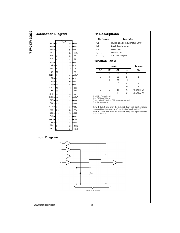
The VCXF162835 low voltage 18-bit universal bus driver bines D-type latches and D-type flip-flops to allow data flow in transparent, latched and clocked modes. Data flow is controlled by output-enable (OE), latch-enable (LE), and clock (CLK) inputs. The device operates in Transparent Mode when LE is held HIGH.
74VCXH162835 Key Features
- I18 O1
- O18 Description Output Enable Input (Active LOW) Latch Enable Input Clock Input Data Inputs 3-STATE Outputs